Moving from another Design Tool
Contents
- Importing Design Files
- The Altium Designer Environment
- Getting Help
- Project-Based Design
- Multi-Channel Design
- Preferences
- PCB Layout and Design
- View Configuration and the Layer Stack Manager
- PCB Board Options - Document Settings
- PCB Board Wizard
- Interactive Routing
- Design Rules
- Signal Integrity
- Mixed-signal Circuit Simulation
- See Also for PCB Design
- Compilation - a Cornerstone of Altium Designer
- Where are my nets and components from my design?
- Configuring Design Connectivity
- Verifying Your Design - Expanded Error Checking
- Design Synchronization
- Components and Libraries
- Where are my libraries? Some Basics on Library Management
- A Brief Note on Database Linking
- Multiple Monitor Support
- Project Outputs
- Altium Designer Viewer
The following links provide tool-specific information to help you move to Altium Designer:
- Cadstar® Importer
- CadSoft® EAGLE® Importer
- Cadence Allegro® PCB Editor
- Mentor Graphics® DxDesigner®
- Mentor® Expedition® Importer
- OrCAD®
- PADS® Layout™ and OrCAD® Capture™
- Moving to Altium Designer from Pads® Logic™ and PADS® Layout™
- P-CAD®
- P-CAD to Altium Designer Terminology Guide
- Protel 99 SE®
This article highlights the key concepts you need to be aware of when moving to Altium Designer from another Design Tool. It identifies Altium Designer's functionality and how to get started - helping you ramp up your productivity and quickly take advantage of this powerful and flexible electronic product development environment.
Importing Design Files
Main article: Importing and Exporting Design Files
One task that has always been a difficult challenge is being able to move electronic product designs from one design environment to another. Whether you have changed design tools or acquired designs from another company, at some stage you will need to import a schematic or PCB design into Altium Designer.
Altium Designer unifies the import process for importing designs from a variety of different design tools. The Importer Wizard walks you through the import process, handling both the Schematic and PCB parts of the project, as well as managing the relationship between them. Launch the Import Wizard from the File menu.
The architecture of the Importing Wizard is designed to allow the easy addition of new importers, without additional complexity for the designer using the system.
The Altium Designer Environment
Main articles: The Altium Designer Environment, Altium Designer Panels Reference
The Altium Designer environment offers a complete electronic product development environment for all areas of design - from schematic capture to the generation of PCB output, as well as complete FPGA design, development and on-chip debugging. The environment is fully customizable, allowing you to set up the workspace to suit the way you work. Consistent selection and editing paradigms across the different editors allow you to easily switch between various designs tasks all within the Altium Designer environment.
Perhaps the single biggest difference that you will notice when you start working in Altium Designer is that there is only one application used to create and edit all design files, regardless of the type of file - schematics, PCB, library, text, and so on. No longer will you have to switch between different applications when you want to move from viewing the schematic to the PCB. All the files (also referred to as documents) open in the same executable, each appearing on a separate document Tab within Altium Designer. As you move from one type of document to another the menus and toolbars automatically switch, giving you the right editing environment for that document.
Getting Help
Main article: Documentation and Help
The best way to learn is through doing, Altium and Altium Designer provide a number of ways to help you do that:
- F1 over any object, editor, panel, menu entry or button to open an article in your preferred browser.
- Shift+F1 while running a command for a list of shortcuts you can use in that command.
- Search the Altium online documentation center, http://techdocs.altium.com/.
- Visit the TRAININGcenter where you can watch over 100 short training videos, each detailing the exact steps needed to completing a task.
- Join a discussion forum and share your thoughts with your industry peers.
Project-Based Design
Main article: Project Management
The starting point for every design created in Altium Designer is a project file. There are a number of project types supported, each targeting a different final implementation, for example PCB project, Library project, FPGA project, Embedded project, Core Project and Script project. The project file stores links to the actual design documents that are part of the project, as well as project-specific settings.
Multi-Channel Design
Main articles: Multi-Channel Design Concepts, Creating a Multi-channel Design, Parametric Hierarchical Design
Complex hierarchy is the general term used throughout the industry to describe the process of using multiple instances of the same sheet in a schematic hierarchy. Traditionally, a design that included complex hierarchy had to go through a process of 'flattening' or 'expanding' the hierarchy at some point, to uniquely instantiate every component and net. Altium Designer does not need to do this, so this multiple-instantiation capability is referred to as multi-channel design instead of complex hierarchy.
The ability to be able to make each channel different by passing parameters to it from the parent sheet symbol is also supported, and is referred to as parametric hierarchy.
Using parametric hierarchy you can parametrically define the component value, supporting the situation where a component does not have the same value in each channel. Parametric components are defined by declaring their value as a parameter of the sheet symbol above, and then referencing that parameter on the target component.
Preferences
Main article: Altium Designer Environment Preferences
Global Preferences are accessed by selecting DXP » Preferences from the menus. The preferences configured here are stored as part of your installation, they do not travel with the design files. File-specific settings, such as schematic document options and printed circuit board options are accessed via the Design menu in each editor.
PCB Layout and Design
Successful board layouts rely on design systems that unify the design definition with the physical layout and routing. Altium Designer offers such a PCB system which includes a number of familiar features to help you place and route your board. When the PCB Editor is active (i.e. a PCB document (*.PcbDoc) is open and active) the main application window will contain:
- A main design window in which you can start designing, capable of display in both 2D and 3D (select in the View menu)
- Menus and toolbars that are specific to the PCB Editor
- Workspace panels that are both global and editor-specific
View Configuration and the Layer Stack Manager
View Configurations are settings that control many PCB workspace display options for both 2D and 3D environments, and apply to the PCB and PCB Library Editors. The view configuration last used when saving any PCB document is also saved with the file.
Select Design»Board Layers & Colors (shortcut: L) from the main menu to open the View Configurations dialog, or switch configurations using the drop down in the main toolbar, as shown below.

To open the Layer Stack Manager select Design » Layer Stack Manager (shortcut D, K) from the menus. The Layer Stack Manager dialog shows the current layer stack up of the board. Signal and plane layers can be added, removed, or their order changed. Double-click on an electric or insulation layer to configure layer properties, such as: thickness, net association (plane layers), or the dielectric constant.
PCB Board Options - Document Settings
All options for the placement grid, measurement units, sheet position, and designator display mode are set in the Board Options dialog. With a PCB document active in the main design window (for this and all of the following context-sensitive dialogs), select Design » Board Options (shortcut D, O) from the menus to open the Board Options dialog.
For multi-channel designs, you can select between logical and physical designator display on the PCB in the Board Options dialog.
PCB Board Wizard
Before you can transfer your design from the Schematic Editor to the PCB Editor, you'll need to have at the very least a blank PCB with at least a board outline. The PCB Board Wizard allows you to easily create a basic PCB design using many industry-standard board outlines as well as create your own custom board sizes. The PCB Board Wizard is launched from the Files panel in the New from template section. At any stage you can use the Back button to check or modify previous pages in the wizard.
Interactive Routing
Main article: PCB Routing
Altium Designer also has interactive routing modes for interactive routing. Modes for interactive routing are not dependent on licensing options, and are all available in the PCB Editor.
Design Rules
Main articles: Design Rules, Creating Design Rules, Design Rule Checking, Scoping Design Rules
Altium Designer's PCB Editor is a rules-driven design environment. You can also transfer your favorite design rules from another board. Design rules can be exported from, and imported to, via the PCB Rules and Constraints Editor dialog, as shown shown below.
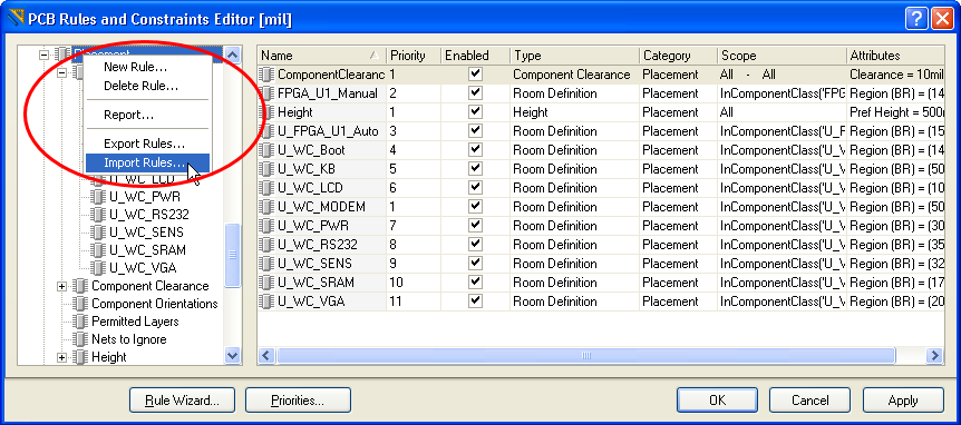
To Import, select Import Rules from the right-click menu, the Choose Design Rule Type dialog will open.
Signal Integrity
Main articles: Performing Signal Integrity Analyses, Signal Integrity Rules, Signal Integrity Panel
In addition to the standard set of design rules for DRC, Altium Designer also supports Signal Integrity analysis, which is integrated directly into the PCB Editor (Tools » Signal Integrity). This includes: pre-layout and post-layout Signal Integrity analysis capabilities that you can perform from either the Schematic or the PCB Editors; evaluate net screening results against predefined tests; perform reflection and crosstalk analysis on selected nets, and display waveforms; and calculate suitable termination values using the termination advisor.
Mixed-signal Circuit Simulation
Main article: Defining & running Circuit Simulation analyses
Mixed-signal circuit simulation is a unified part of the capture process, and is fully integrated with the schematic editing environment. Before you launch the Mixed-signal circuit simulation, make sure that any schematic sheet within the project is open. Simulation models need to be associated with every component in the schematic document before simulation can be launched from the command Design » Simulate » Mixed Sim. Simulation is done for the entire project.
See Also for PCB Design
Here's some ideal starting articles to learn more about PCB Design in Altium Designer:
- Tutorial - Getting Started with PCB Design
- Editing Multiple Objects to learn about editing the the Find Similar Objects functionality
- PCB Inspector Panel which displays the common properties of different objects and lets you filter and edit them
- PCB Object Reference
- Preparing the Board for Design Transfer
Compilation - a Cornerstone of Altium Designer
Compilation is a cornerstone concept of the Altium Designer environment. Compilation is a process that allows you to harness many powerful design features.
When you select Project » Compile Project the compilation process works out the structural relationships between the source schematic (or HDL) documents in the project, then determines the net-level connectivity within each sheet, and finally the connectivity between the sheets. All this component and connective intelligence from your schematics design is written into an internal data structure that can then be used for many post-compilation activities, such as comparing and showing differences between schematics, parameter managing, parametric navigation of your design, cross probing back and forth between the schematics and PCB, and much more.
Where are my nets and components from my design?
Connectivity is not as explicit in your design as it was before, but rather has to be extracted from the design using the compilation process. This is available through the right-click menu in the Projects panel, or using the Project » Compile Project menu command.
Once the design is compiled the sheet-level hierarchy, as well as all the components, nets and buses are displayed in the Navigator. From here you can easily locate any component, bus, net or pin throughout the entire design. And if you hold the Alt key as you click on an object in the Navigator it is highlighted on the PCB as well as the schematic – no longer will you need to inspect net lists to review design connectivity.
Configuring Design Connectivity
Main article: Connectivity and Multi-Sheet Design
Altium Designer supports different types of design connectivity, and this must be set to suit the structure of the design. The type of sheet-to-sheet connectivity is called the *Net Identifier Scope. This is defined in the Options tab of the Options for Project dialog and saved with the project. From the Project menu select the Project Options command, and go to the Options tab.
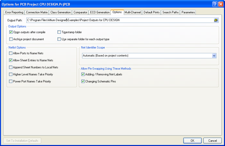
The Net Identifier scope is set in the Options tab of Project Options
In the Net Identifier Scope dropdown you can select from the following connectivity options:
- Automatic (Based on project contents)
- Flat (Only ports global)
- Hierarchical (Sheet entry <-> port connections)
- Global (Net labels and ports global)
The Import Wizard handles connectivity automatically through the translation process and will give you the Automatic (Based on project contents) configuration by default. Hierarchical blocks are mapped as sheet symbols, and they will translate to sheet symbols in Altium Designer. In Automatic mode, the design compiler then looks at the sheet symbols on the top sheet. If there are sheet entries (hierarchical pins) in them, it will assume vertical connectivity, and internally use the Hierarchical option. If there are no sheet symbols on the top sheet, or if there are sheet symbols but they do not include any sheet entries, it will assume horizontal connectivity for which there are two ways that Altium Designer supports this: Flat and Global. In order to determine which of these two options to use, the design compiler looks for ports or off-sheet connectors on the subsheets. If there are any it uses the Flat option, if there are no ports it uses the Global option.
You can easily go back and change the configuration after translation through the Project Options dialog from the Projects menu.
Verifying Your Design - Expanded Error Checking
Main articles: Project Compiler Violations Reference, Compile Errors
Another benefit that results from compiling a project in Altium Designer is built-in error reporting. This is completely configurable for your needs and can be done before your project is compiled. Right-click either on the project file and invoking the Project Options command, or also through the Project menu.
You may wish to get a better picture of the entire development cycle and how it unfolds from an engineer's perspective by reading An Overview of Electronic Product Development in Altium Designer
Design Synchronization
Main article: Finding Differences and Synchronizing Designs
Design synchronization is fully integrated in Altium Designer, without the need for passing a netlist. Synchronization in Altium Designer is also bi-directional, allowing you to make annotation changes and component property updates in both directions between your schematic and PCB, in a single operation.
Components and Libraries
Main article: Component, Model and Library Concepts
Altium Designer supports working directly from the source symbol or model libraries, an ideal approach when the schematic and PCB are designed by separate organizations.
The logical symbol is assumed to be the essential starting point of a component. It can be initially defined at minimum as a name in a schematic library to which pins and any graphical symbols or alternative display options needed for implementation may be added. This flexibility allows a component to be represented in different ways during the design and capture process. This may not only be as a logical symbol on the schematic, but also be a footprint on the PCB or even as a SPICE definition for simulation.
Where are my libraries? Some Basics on Library Management
You'll be able to view your source schematic and PCB library files immediately after translation through the Projects panel. Your translated libraries are automatically grouped into one PCB project.
Libraries are installed (added) to the Altium Designer environment, making their components available in all open projects. Display the Libraries panel, from there you can install and remove libraries. Libraries can also be linked to any project, and you can also define project search paths, useful for referencing simulation models.
See Enhanced Library Management Using Integrated Libraries for a further discussion on using Integrated Libraries.
A Brief Note on Database Linking
Main articles: Linking Existing Components to Your Company Database, Using Components Directly from Your Company Database
Appreciating the fact that many designers like to link from the components in their electronic design software to their company database, Altium Designer has strong support for linking and transferring database data through the design process and into the Bill of Materials.
Two techniques are supported, one where the Altium Designer library symbol holds all model references and also includes links into an external database, the second where the database holds all model references and other company information. While database connections in Altium Designer are set up for MS Access databases (*.mdb files) by default, any ODBC-compliant database can be accessed.
Multiple Monitor Support
Altium Designer has full support for multiple monitors. If you have multiple monitors on your PC you can easily drag a document out of Altium Designer and drop it on the second monitor, greatly enhancing your design productivity. Multi-monitor support is configured in Windows.
Project Outputs
- To learn about generating manufacturing output, either using the OutputJob Editor or using the Reports menu, see Design to Manufacturing
- To learn about the CAM Editor see Auto-Loading Fabrication Output into the CAM Editor
- To learn about the built in PDF generation wizard, see Smart PDF available from the File menu and Publish to PDF available in the Output Job Editor
Altium Designer Viewer
Main article: Altium Designer Viewer
Altium Designer Viewer provides quick, easy, and secure read-only exploration of design projects and documents that have been created using Altium Designer. Users can view, print and interrogate all aspects of a design created by Altium Designer, making design data more accessible through the entire design-chain. The Viewer not only enhances collaboration within an organization, but also between the design team and external parties, greatly improving design work flow and project productivity.
The Altium Designer Viewer can be freely downloaded and does not require a license.