Moving to Altium Designer from Pads Logic and PADS Layout
Contents
- Getting Started - Transferring Your PADS Logic Designs
- Importing Which PADS ASCII Logic Files?
- Using the Import Wizard for PADS Logic Files
- Getting Started - Transferring Your PADS Layout Designs
- Importing Which PADS Layout Files
- Using the Import Wizard for PADS Layout Files
- Layer Mapping for PADS PCB ASCII Files
- Getting Started - Transferring Your PADS Library Files
- Importing which PADS PCB Library Files
- Importing Which PADS Schematic Library Files
- Using the Import Wizard for PADS Library Files
- Layer Mapping for PADS ASCII Library Files
- The Altium Designer Environment
- Working with Documents
- Sheet Structure in PADS Logic
- Defining Net Connectivity
- The Schematic Symbol is the Part
- Design Rule Categories
- Design Rules Scoping
- Altium Designer Libraries
- See Also
Translating complete PADS® Logic™ and PADS® Layout™ designs, including PCB, Schematic files and library files can all be handled by Altium Designer's Import Wizard.
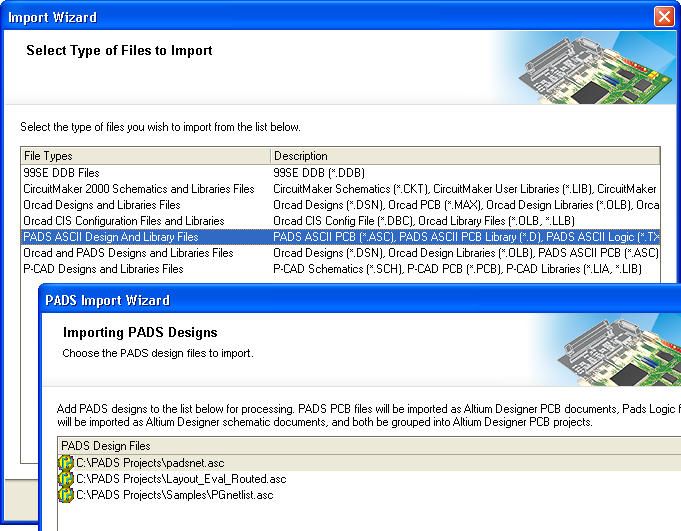
Import Wizard PADS ASCII Design and Library files.
The Import Wizard streamlines the design translation by analyzing the PADS design files and offering defaults and suggested settings for project structure, layer mapping, PCB footprint naming, and so on.
The Import Wizard only translates PADS ASCII versions 5.2 onwards and does not read PADS binary files. If you only have binary PADS files you will need to export these binary files into ASCII format from your PADS application, preferably in the ASCII 2005.2 format.
The PADS designs imported by the Import Wizard are captured as documents in individual PCB Projects which are created automatically after the translation in Altium Designer. Errors in the translation are reported in a log file with the filename of the imported design with a LOG extension as shown in the Reporting Options page of the PADS Import Wizard as in the figure below.
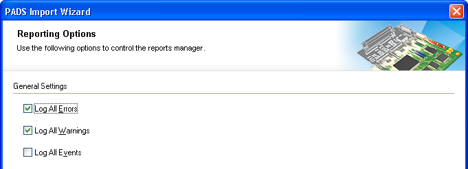
Import Wizard - Reporting Options to control the reports manager.
We will go through the import process in three sections; importing PADS logic designs, importing PADS Layout files and importing PADS Library files below.
Getting Started - Transferring Your PADS Logic Designs
Translating complete PADS Logic designs which are Schematic files can be handled by Altium Designer's Import Wizard. The Import Wizard streamlines the design translation by analyzing your files automatically. One Altium Designer schematic document is generated for each PADS Logic sheet within a Logic file by the Import Wizard. Each translated Logic file will be grouped into automatically created Altium Designer PCB project with an *.PrjPCB file extension.
Files in the Import Wizard translate as follows:
- PADS ASCII Schematic Logic sheets within a Logic file with an *.TXT extension translate to Altium Designer Schematic files with an *.SchDoc file extension.
Importing Which PADS ASCII Logic Files?
The Import Wizard supports Pads Logic versions 2005.0 and 2005.2 as well as the older Pads PowerLogic version 5.2. It is best to export Logic files that have the version 2005.2 as they contain the most data. These files have to be in ASCII format. The file extension used by the Pads ASCII format is *.txt.
For the import of PADS Logic files, there are no specific settings in the Import Wizard in Altium Designer.
Ensure that when the Logic ASCII files are exported from the PADS application; enable all Logic data sections in the ASCII Output dialog in PADS application as shown in the figure below.

Export the PADS Logic file with the appropriate sections enabled in the PADS application.
All the data for translation needs to be in the ASCII file, which is why Decals, Part Types and Parts must all be enabled otherwise no components will be imported. Thus the Decals section need to be enabled for Part Types section and the Part Types section needs to be enabled for Parts section as well.
In some cases, you can skip some of the above settings such as Text and Lines which are usually used for the border and title blocks. You can use Altium Designer's Schematic border and title blocks instead.
The Schematic designs normally do not require any libraries, and in fact doesn't use them. Currently the Plot Params section and the Rules section within a PADS file are ignored when files are being imported into Altium Designer.
Using the Import Wizard for PADS Logic Files
The Import Wizard can be launched from the Altium Designer File menu. Click on this menu command to invoke the wizard. Right-click pop-up menus are available for further control over the translation process through each page of the wizard.
Make sure you firstly export your PADS Logic files as ASCII files in the 2005.2 version. Incompatible or incorrect file formats are not imported and an error file with a LOG extension will be generated.
Once the PADS Logic files have been added in the Import Wizard's PADS Design Files list within the Importing PADS Designs page, you can toggle the options to control the Reports manager, review the output project structure and then specify the output directory to import the files in Altium Designer. Each PCB project is created for each PADS Logic schematic file in Altium Designer.
Getting Started - Transferring Your PADS Layout Designs
PADS Layout ASCII File Export format.
Translating complete PADS Layout designs which are PCB files can all be handled by Altium Designer's Import Wizard. The Import Wizard removes much of the headache normally found with design translation by analyzing your files and offering many defaults and suggested settings for project structure, layer mapping, PCB footprint naming, and so on. Complete flexibility is found in all pages of the Wizard, giving you as little or as much control as you would like over the file translation settings, before committing to the actual translation process.
Importing Which PADS Layout Files
There are different PCB file formats that can be exported from the PADS Layout package version 2005 and they are;
- PADS Layout V2005.2
- PADS Layout V2005.0
- PADS PowerPCB V5.0, V4.0, V3.5, V3.0 etc
Since AD10 Update 6 - V2007.0
- 9.x up to V9.5
Schematic and PCB Designs, and Schematic and PCB libraries.
The Units list has two settings, Basic and Current units. The Basic setting causes the ASCII file to be in the database units. The Current setting exports units based on the design setting, which can be mils, mm, or inches.
The Expand Attributes section has two settings; Parts and Nets. Checking either of these setting causes higher level attributes to be propagated into and exported with either the Parts or Nets or both depending on what is checked.
The Sections part of the dialog has a list of PADS objects that can be in an ASCII file. A PADS PCB ASCII file is divided into sections as outlined below which is taken directly from the PADS Help.
| Item | Exported information |
|---|---|
| PCB Parameters | Global design information, such as units and colors |
| Reuse | Elements in, and the definition of, a physical design reuse |
| Text | Text |
| Lines | Two-dimensional lines |
| Clusters | Clusters and unions |
| Vias | Vias and dangling vias, jumpers, and pad stacks |
| Decals | Footprints |
| Packages | Electrical information |
| Parts | Component instances |
| Jumpers | Jumpers If you plan to export to the PowerPCB V1.1 ASCII format, you cannot output complete jumper information. This is because PADS Layout considers jumper pins as vias and jumpers are exported as vias when you select the Vias check box. |
| Connections | Unrouted pin pairs |
| Routes | Traces, including route loops |
| Teardrops | Must export routes if you want to export teardrops. If you plan to export to the PowerPCB V1.1 ASCII format, you cannot output teardrops. |
| Miscellaneous | Information not included in other items |
| Rules | Clearance, routing, and high-speed rules |
| CAM | Information related to plot file configurations generated using CAM |
| Pour | Copper pours |
| Assembly Options | Assembly variants |
| Test Points | Test points and the test side (top, bottom, or both) |
| Attributes | Attribute Dictionary and all individual attributes and value assignments in the design. Status of attributes (read-only, system, ECO-registered, or hidden). |
Using the Import Wizard for PADS Layout Files
The Import Wizard can be launched from the Altium Designer File menu. Click on this menu command to invoke the wizard. Right-click pop-up menus are available for further control over the translation process through each page of the wizard. These translated files will be grouped into an automatically created Altium Designer PCB project (*.PrjPCB).
Files in the Import Wizard translate as follows:
- PADS ASCII PCB Layout (*.ASC) files translate to Altium Designer PCB files (*.PcbDoc).
Layer Mapping for PADS PCB ASCII Files
All used PADS PCB layers must be mapped to an Altium Designer layer prior to import when using the Import Wizard. There are additional options provided to control the automatic creation of design rules, missing vias and keep-out conversions as well.
Use the Layer Mapping Options from the Edit Mapping button in the Import Wizard to associate PADS PCB layers to Altium Designer layers.
It should be noted about how the layers are mapped on import for PCB designs. Layer Mapping is a mapping between the names of the PADS PCB layers and Altium Designer PCB layers. You can change as many mappings as you want as only suggested default mappings are given. This mapping is used by the Import Wizard to build the layer mapping for each PCB that can then be individually customized. The rationale here is that should you wish to import ten PCB designs and you want to map the layer Assembly 1 to Mechanical Layer 1, you would not have to customize each of the ten PCB designs in order to get the right layer mapping. The customized layer mappings are stored in a .INI file.
The advantage to importing in this manner is that batch management of layer mapping saves time when importing multiple designs. In this instance, the default layer mapping will be saved to your Preferences. The disadvantage to using this is that Default Layer Mapping is not always intelligent with differing structures in designs, so some manual changes may be needed.
Turning the Override Pad Inner Value option on means that imported pads will have their sizes on the midlayers set to the largest size found
Make sure you firstly export your PADS Layout files as ASCII files in the 2005.2 version. Incompatible or incorrect file formats are not imported and errors are stored in a text file with a LOG file extension.
Once the PADS Layout files have been added in the Import Wizard's PADS Design Files list within the Importing PADS Designs page, you can toggle the options to control the Reports manager, review the output project structure and then specify the output directory to import the files in Altium Designer. Each PCB project is created for each PADS Layout PCB file in Altium Designer.
Getting Started - Transferring Your PADS Library Files
Translating complete PADS library files can all be handled by Altium Designer's Import Wizard. The Import Wizard removes much of the headache normally found with design translation by analyzing your files and offering many defaults and suggested settings.
Complete flexibility is found in all pages of the wizard, giving you as little or as much control as you would like over the file translation settings, before committing to the actual translation process. Each translated library file will be imported into an automatically created Altium Designer PCB project (*.PrjPCB).
The PADS application (Logic and Layout) both support four library types; (Decal, Part, Lines and CAE Decal files) however the Import Wizard can only translate three library types - Decal library, Part library and CAE Decal library only.
Importing which PADS PCB Library Files
The PADS package exports a decal library with footprint definitions in ASCII format using the file extension *.d. The conversion is very straightforward with the Import Wizard in Altium Designer; a PADS decal file is translated into an Altium Designer library document of PCB footprints. It is highly recommended to import the 2005.2 version PCB decal files (ASCII format).
Importing Which PADS Schematic Library Files
The PADS Logic package exports the Schematic symbols as CAE decals in ASCII format with the file extension *.c. This file only contains the definitions of the Schematic symbols, such as the graphics and pin orientation. The CAE files alone cannot be used to translate into Altium Designer Schematic components. A Schematic library component in Altium Designer is the "combination" of the PADS Logic symbol and component information such as gates and pin designator. The PADS package exports the specific component information into a file called "Part Library". It is an ASCII format file with the extension *.p.
You have to supply the Part Library (*.p) and CAE Decal (*.c) files in order to translate into an Altium Designer Schematic library. The CAE decal (*.c) files are used as a lookup for CAE (or symbol) definitions. The user can supply as many *.c and *.p files and add them in the Import Wizard, which will try to look up the gate name (CAE name) for the part reference.
The best way to smoothen the Import Wizard in Altium Designer process is to supply the set of CAE files (*.c) that have the CAE definitions that the parts (*.p) reference. For example, you can export the common libraries into the common.c file and add them into the Import Wizard.
Using the Import Wizard for PADS Library Files
Layout decal library files have a *.d file extension.
Logic CAE decal library files have a *.c file extension.
Logic/Layout Part Type library files have a *.p file extension.
The Import Wizard (can be launched from the Altium Designer File menu. Click on this menu command to invoke the wizard. Right-mouse click command menus are available for further control over the translation process through each page of the wizard.
PAD ASCII libraries with PCB decals (\*.d), CAE decals (\*.c) and Parts (\*.p).
Files in the Import Wizard translate as follows:
- PADS ASCII Library PCB decal files (*.d) as Altium Designer PCB library files with a *.PCBLIB file extension.
- PADS ASCII Library CAE decal files (*.c) and PADS ASCII Library Part Type files (*.p) as Altium Designer library files with a *.SCHLIB extension.
Layer Mapping for PADS ASCII Library Files
All used PADS PCB layers must be mapped to an Altium Designer layer prior to import when using the Import Wizard. There are additional options provided to control the automatic creation of design rules, missing vias and keep-out conversions as well.
It should be noted about how the layers are mapped on import for PCB designs. Layer Mapping is simply a mapping between the names of the PADS PCB layers and Altium Designer PCB layers. You can change as many mappings as you want as only suggested default mappings are given. This mapping is used by the Import Wizard to build the layer mapping for each PCB that can then be individually customized. The rationale here is that should you wish to import ten PCB designs and you want to map the layer Assembly 1 to Mechanical Layer 1, you would not have to customize each of the ten PCB designs in order to get the right layer mapping. The customized layer mappings are stored in a .INI file.
The advantage to importing in this manner is that batch management of layer mapping can save a lot of time when importing multiple designs. In this instance, the default layer mapping will be saved to your Preferences. The disadvantage to using this is that Default Layer Mapping is not always intelligent with differing structures in designs, and so some manual changes may be needed afterwards. You'll need to decide what is best for your situation.
Once the PADS library files have been added in the Import Wizard PADS Design Files list within the Importing PADS Designs page, you can toggle the options to control the Reports manager, review the output project structure and then specify the output directory to import the files in Altium Designer. Each PCB project is created for each PADS library file in Altium Designer. Remember a set of* .p and its corresponding *.c files is treated as a translated single library file in Altium Designer.
The Altium Designer Environment
In PADS Layout all design work begins on the workspace, the logical working area of the PCB design. Each design is saved to a single design file (*.PCB file). In PADS Logic, all design work begins on the sheet, the logical working area of the schematic design. There can be multiple schematic sheets within a single PADS schematic design file (.SCH file).
Working with Documents
In Altium Designer, the logical design area begins with a document, and for each document there is a file stored on the hard drive. This means that for each Altium Designer schematic sheet there is a file. This is an important conceptual difference to remember. There can also be multiple design documents of varying types, depending on the nature of the design you are working on in Altium Designer. Getting started, most PADS users will be interested in the schematic and PCB document types as these are the files that their designs will be translated to.
Sheet Structure in PADS Logic
Like Altium Designer, PADS Logic supports flat and simple hierarchical designs. Both use a block-like symbol to define sheet-to-sheet structure in a hierarchical design, called a Sheet Symbol in Altium Designer, and a Hierarchical Block in Logic. In both, the symbol references the lower level schematic. In Altium Designer this is another schematic sheet.
Typically a flat Logic design is one schematic (folder), with the design being drawn on as many pages as required in that schematic (folder). For a hierarchical design, the hierarchical block symbol (or part with an attached schematic sheet or model) is the mechanism used to partition the major functional regions of a design.
For a simple hierarchy, each hierarchical block, or part with an attached schematic folder represents a unique design module.
Defining Net Connectivity
In PADS Logic, net connectivity is made using off-page symbols, hierarchical symbols and globals. Nets between schematic pages within a single schematic folder are connected through the off-page symbols while the hierarchical symbols connect the nets between the schematic folders. Globals are used to connect power/ground nets throughout the design.
Altium Designer uses a similar set of net identifiers to create net connectivity. Within a schematic sheet you can use Wires and Net Labels. Between schematic sheets, nets in a flat design are typically connected using Ports, but Off-Sheet Connectors are also available. Nets in a hierarchical design are connected from a Port on the lower sheet to a Sheet Entry of the same name, in the sheet symbol that represents the lower sheet. Power/ground nets are connected using Power Ports.
The Schematic Symbol is the Part
As an expert PADS Layout user, you'll know that parts form the basic building blocks of design in PADS Layout. Parts are defined as having a part type, a logic family, number of pins, number of gates, and signal pins. The term component is only used when the part becomes placed as a physical object in the PCB layout design.
In PADS Layout (PCB), a part can represent one or more physical components. Parts in PCB designs usually correspond to physical objects: gates, chips, connectors, objects that come in packages of one of more parts. Multiple-part packages are physical objects that are comprised of one or more parts.
In PADS Logic, a part is a logical entity that is described graphically by a symbol, pins and various properties. As parts are placed in a schematic design, Capture maintains the identity of the part for back annotation, net listing, bills of materials, and so forth. At the very minimum, a part requires a part name, a part reference prefix, and a name of a PCB footprint.
These two definitions that use the same term depending on the context of design may initially cause some confusion in the new environment which uses the term component. But it is not unlike how things work in Altium Designer except that the schematic symbol is effectively the part for all phases of design, and not just the PCB Layout portion of it.
In Altium Designer, the logical symbol is assumed to be the essential starting point of a component. It can be initially defined at minimum as a name in a schematic library to which pins and any graphical symbols or alternative display options needed for implementation may be added. This flexibility allows a component to be represented in different ways during the design and capture process. This may not only be as a logical symbol on the schematic, but also be a footprint on the PCB or even as a SPICE definition for simulation.
Design Rule Categories
True to the unified nature of Altium Designer, which incorporates all phases of electronic design, design rules are accessed from a single dialog - the PCB Rules and Constraint Editor. There are 10 rule categories that cover all respective aspects of design verification.
| PADS Layout Rule Category | Altium Designer Rule Category | Comments |
|---|---|---|
| Clearance | Placement | Room Definitions, Component Clearances, Component Orientations. Permitted Layers, Nets to Ignore, and Component Height. |
| Routing | Routing | Differential pairs routing can be checked from within the PCB Editor. |
| High Speed | High Speed | Matched Net Lengths, Length and parallel segments. All rules easily checked between layout and the schematic without importing. |
| Electrical | Integrated into Altium Designer's PCB Editor. | |
| Fabrication | Manufacturing | Verified within the PCB Editor environment using the CAM Editor. Minimum Annular Ring, Acute Angle, Hole Size, and Layer Pairs. |
| SMT | SMD To Corner, SMD To Plane, and SMD Neck-Down. | |
| Plane | Power Plane Connect Style, Power Plane Clearance and Polygon Connect Style. | |
| Mask | Solder and Paste Mask Expansion | |
| Test Point | Test Point | Styles and usages |
| Signal Integrity | In addition to standard set of design rules for DRC, signal integrity analysis is integrated directly into the PCB Editor (Tools»Signal Integrity). |
A table of the more commonly-used PADS Layout design rules terms and their closest respective Altium Designer equivalents (* indicates that this rule is not checked as a part of the core design rules in PADS Layout).
Design Rules Scoping
It may arise that a design object is covered by more than one rule with the same scope. In this instance, a contention exists. All contentions are resolved by the priority setting. The system simply goes through the rules from highest to lowest priority and picks the first one who's scope expression (s) matches the object(s) being checked.
Rules Scope - the extent of a rule's application - replaces the Rules Hierarchy from PADS Layout. A scope is effectively a query that you build to define all the member objects that are governed by that rule, giving you full control.
For the sake of a baseline comparison, let's review the Rules Hierarchy of PADS Layout. These rules rely on a pre-defined list format where higher numbers on the list have precedence over those that are lower:
- Default
- Class
- Net
- Group
- Pin Pair
- Decal/Component
In the PADS Layout rules schema, Default rules are considered level 1 and are the lowest while Decal and Component rules represent the highest. Conditional layer rules can be applied for an additional level of precedence. For example, a Default with a conditional layer rule would be higher in the precedence hierarchy than a simple Default rule.
In Altium Designer, scoping allows you to decide exactly what a rule's precedence will be and how it will be applied to target objects through a query. You can even define multiple rules of the same type, but each targeting different objects. Queries are easily accessed for any rule. Advanced (Query) options are also available to help you write your own, more complex queries.
Double-clicking on any rule while in the PCB Rules and Constraint Editor dialog will bring up the specific query for that rule in the right pane.
If you do not want to use a design rule, but may want to use it in the future, rather than delete it, you can disable it. Toggle the corresponding Enable option for the rule in the relevant list.
All default design rules have a scope (Full Query) of ALL, meaning that they apply to the whole board.
In addition to scoping, there is also a user-defined priority setting (described below). The combination of rule scoping and priority is very powerful and gives an unprecedented level of control that allows you to precisely target the design rules for your board.
Altium Designer Libraries
An integrated library in Altium Designer is one where the source symbol, footprint, and all other information (e.g. SPICE and other model files) are compiled into a single file. During compilation checks are made to see how relationships are defined, to validate the relationship between the models and the symbols and to bundle them into a single integrated library. This file can not be directly edited after compilation, offering portability and security.
All of Altium Designer's 70,000+ components are supplied in integrated libraries, from which the source libraries can be extracted at any time if required.
| PADS Object | Altium Designer Object | Comments |
|---|---|---|
| Decal | Footprint | Graphical representation of the shape defined for the component to mount onto the PCB. This is 2-dimensional representation only, and can be quite different from the actual component itself |
| Part | Part/Component | The term Part is used only as part of the design capture (schematic) process in Altium Designer. Once placed as a footprint into a PCB file, it is given a designator and value (comment) and becomes a component. |
| Lines | Lines | Primitive object used for graphical information. |
| CAE Decal | Schematic symbol | The graphical representation of a schematic part, such as a NOR gate. |
A table of the more commonly-used PADS Library terms and their closest respective Altium Designer equivalents.
See Also
Below are references to other articles and tutorials in the Altium Designer Documentation Library that talk more about the conceptual information as well as walking you through specific tasks. Remember, you can also browse through the Help contents, and use F1 and What's This at any time in a dialog for more details.
For more PCB project options, refer to the tutorial, Getting Started with PCB Design.
For more FPGA project options, refer to the tutorial, Tutorial - Getting Started with FPGA Design.
For a tutorial that steps you through all the basics of creating components, read Creating Library Components Tutorial.
For a tutorial that steps you through all the basics of editing multiple objects, read Editing Multiple Objects.
For an overview of Altium Designer's FPGA design, development and debugging capabilities, read Soft Design.