Editing Multiple Objects
Contents
- Selecting Multiple Objects
- Inspecting the Objects
- Editing the Objects
- Editing Group Objects
- Step 1. Selecting the Capacitors
- Step 2. Changing the Comment String
- Step 3. Adding a New Parameter to the Component
- Step 4. Setting the Voltage Parameter to be Visible
- Applying an Edit to Different Types of Objects Globally
- Changing the Net Name for Existing Routing
- Changing the Layer Property of Different Objects
- Locking Design Objects
- Locking Design Objects on Schematic Sheets and PCB Documents
- Managing Footprints Across the Entire Design
- Using a Query to Find and Edit Multiple Objects
- Filtering to Find the Objects
- Editing Design Objects in the Schematic Library List Panel
- Using a Spreadsheet Program to Edit Design Data
- Creating and Editing Data as you Paste from a Spreadsheet or Table
- Filtering Objects in the Design Workspace - How does it work?
- Tips for Writing Queries
Electronic design is the process of capturing a logical design in the schematic, then representing that design as a set of objects in the PCB workspace. Even for a small circuit, the schematic can include many components, each with numerous models and parameters, and the PCB workspace can also contain a large number of design objects that make up the board. During the course of the design process, the properties of these objects need to change as the designer works to balance out the various design requirements.
To support the task of editing many objects, each version of Altium design tools has included a feature often referred to as Global Editing. The name describes an editing ability, rather than a specific feature or button. In early versions the approach was to edit one object, and then push those changes onto other objects. With the introduction of the DXP integration platform, the technique for applying an edit globally changed.
The basic approach to editing multiple objects now is:
- select the objects to be edited,
- inspect their properties, and then
- edit them.
Keeping this select – inspect – edit sequence in mind, let's look at some examples how you actually do that in the software.
This article describes various techniques for applying edits to multiple objects in your design. It covers using the combination of the Find Similar Objects dialog and the Inspector panel, as well as the Parameter Manager and the Model Manager. Finally, it introduces queries and the List panel, a powerful technique for finding and editing design objects.
Selecting Multiple Objects
There are actually a number of ways of selecting objects, for example the Windows standard mouse click shortcuts can be used. This approach is ideal when the number of objects to be selected is small, or perhaps when there are different kinds of objects to be edited simultaneously.
To select many objects, including over a number of schematic sheets, you can use the Find Similar Objects dialog. To open this dialog, right-click on one of the objects to be edited, and select Find Similar Objects from the context menu.

Right-click and select Find Similar Objects.
Let's walk through the process using an example. Let's say we need to change the name of a power net in the schematic from VCC to 3V3. The name of the power net is defined by the Net attribute of the Power Port object. To change the name, all of the VCC power ports on all of the schematic sheets need to have their Net attribute changed. The first step is to find a VCC power port on the schematic, right click on it, and select Find Similar Objects from the context menu.
Properties of the current object loaded into the Find Similar Objects dialog
The image above shows the Find Similar Objects dialog after right-clicking on a schematic Power Port. It is important to note that the dialog lists the properties of the object you clicked on, so the contents of this dialog will be different if you clicked on something else. You can see that the dialog has two columns, the column highlighted in the image shows the current properties of the object you clicked on – down the bottom you can see that the net name Text is currently VCC.
The second column in the Find Similar Objects dialog is where you configure how to match other objects. For each property of the object, you instruct it to match target objects when this property value is the Same, match when the target has a Different value, or set it to Any when you are not interested in matching by this property.
Note that in in the image below, the matching will occur when the Object Kind is the Same, and when the net name Text is the Same. Or to say that another way, match when the other object is a Power Object with a net name of VCC .
Which properties should be used to match by? In this example the matching is by Object Kind and Text (net name).
The next step is to set the scope of the find action, should it be on the Current Document only, or all Open Documents. In the image below, you can see that this has been set to Open Documents. For this editing action to apply to all the sheets in the project, they must be opened first.
What documents should this edit apply to?
The final step is to define what should happen after all the Power Objects that have net name Text of VCC, in all Open Documents have been found. The image below shows the settings that need to be set for this edit operation.
The key options to be set are:
- Select Matching (to select all the Power Objects with net name Text of VCC ), and
- Run Inspector, which will open the Inspector panel with the selected objects loaded into it.
Click the OK button to select the matching Power Ports. Alternatively, you can use the Apply button, this will select the matching power ports and open the Inspector, but the Find Similar Objects dialog will remain open too – use this approach if you are not sure you have the correct matching criteria.
What should be done with the found objects? Here they are being selected and loaded into the Inspector panel.
Inspecting the Objects
The SCH Inspector shows the properties of the selected objects
Both the schematic and PCB editors include a panel called the Inspector. The basic behavior of the Inspector is that it lists the properties of all objects that are currently selected. The set of selected objects can be the same kind of object - for example the image above shows the properties of ten power ports - or they can be different types of objects.
Properties that are identical for all the selected objects have their value displayed, for example all ten power ports currently have the same Color, the same Orientation, the same Style and the same Text (net name).
For each power port property that has a different value, you will see <...> instead, for example the X1 location. This means that not all these ten objects have the same X1 value, which makes sense since they each have a different location.
Note in the image above that the SCH Inspector includes two options at the top. It is important that you set the second of these, which sets the display of where the found objects are from – from the current document, open documents, or open documents of the same project. To have all of the selected power ports loaded into the SCH Inspector you must set this to open documents or open documents of the same project.
Editing the Objects
Editing the net name Text
So far you have selected the Power Objects you want to edit, inspected their properties in the Inspector, you are now ready to edit them.
When you click to edit the net name text, the text selects ready to edit, simply type in the new value. The ... browse button appears at the end of the Text field, click this when you want to perform a partial string substitution. For this edit, we will be replacing all the text, so we simply replace the entire contents of the cell with the new text, 3V3.
The change you make to the text value is applied to all the selected objects as soon as you press ENTER on the keyboard, or click another cell in the SCH Inspector.
If you change your mind during the edit, press the ESC key on the keyboard to abort the edit. To Undo an edit that has been applied, select Edit » Undo from the menus. If the edit has been applied to multiple schematic sheets, you will need to perform an Undo action in each sheet.
The image below shows the SCH Inspector panel after changing the text and pressing ENTER, next to one of the edited power ports.
One of the ten updated power ports.
You can use this approach to apply an edit globally to any type of object in the Schematic or PCB Editors.
After performing the edit, you will probably find that all the other objects on the schematic are faded out, or masked. While something is masked it cannot be edited, to remove the mask click the Clear button at the bottom right of the workspace shortcut: Shift+C).
Editing Group Objects
The edit that we just performed was on a primitive object, that is, one of the basic objects used in the Schematic Editor. More complex objects, such as components, are called group objects; these are essentially a collection of primitive objects. For example, a component on a schematic is a collection of drawing objects, strings, parameters, pins, and references to models. The primitive objects that belong to a group object are sometimes referred to as the child objects, and the group object is their parent object.
Let's look at a typical group object edit that you might want to perform. Your design includes several 470uF 16V capacitors, using the footprint MCCT-B. Currently the voltage is specified as part of the components' comment string. You need to change this and specify the voltage as a component parameter instead, and make this parameter visible on the schematic.
The steps we need to perform are:
- Select capacitors with a value of 470uF 16V , and MCCT-B footprint.
- Change their comment to be 470uF (remove the 16V text).
- Add a new parameter to these components, with a name of Voltage, and a value of 16V.
- Change the visibility of this parameter so its displayed on the schematic.
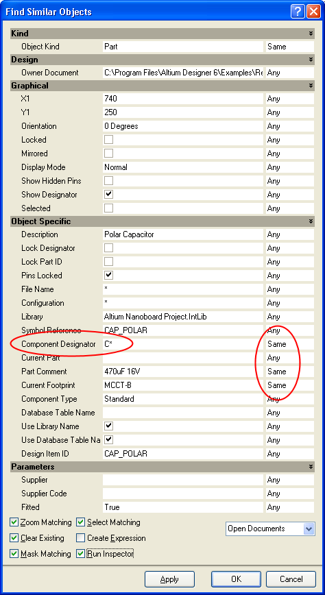
Finding the 470uF 16V capacitors
While this might seem a complex set of edits to perform in one go, it is actually quite straightforward.
Step 1. Selecting the Capacitors
To select all the 470uF 16V capacitors, right-click on the component symbol of one of them and select Find Similar Objects from the context menu.
We will use the approach covered in the previous example, except this time you want to match on components that have the same Part Comment , and the same Current Footprint, as shown in the image above.
Note that we can also match on components that have a designator starting with the letter C. This is done by changing the component designator value in the Find Similar Objects dialog from what it opened as, to C* (above). Click OK to select the matching capacitors.
Step 2. Changing the Comment String
The view after performing a Find Similar Objects, showing the matching capacitors found on this sheet
After running the Find Similar Objects dialog, the SCH Inspector panel opens (if the Run Inspector option in the Find Similar Objects dialog was enabled). Behind it will be the schematic sheet displaying the matching objects selected on that sheet. If the Zoom Matching and Mask Matching options were enabled in the Find Similar Objects dialog, then the view would be zoomed and all the objects that did not match would be faded, or masked out.
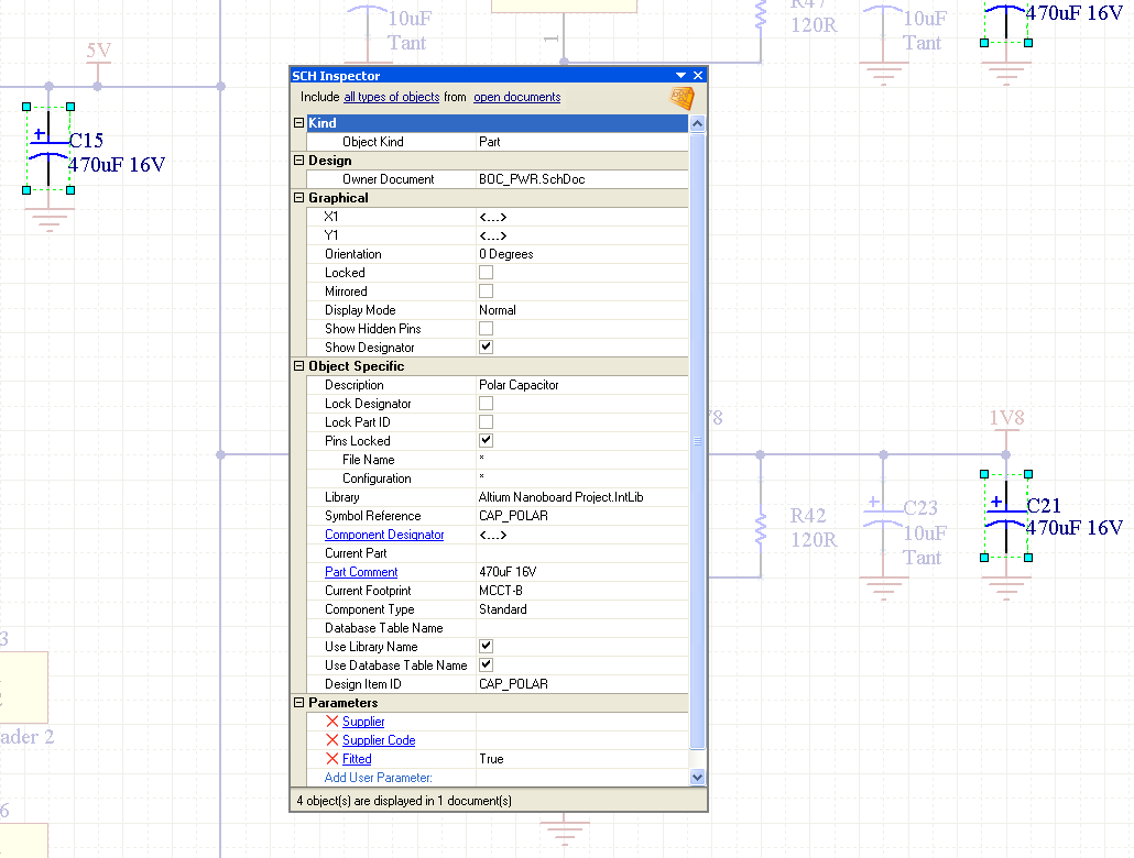
The image above shows the results. There are four capacitors found on this current schematic sheet.
You can check the status line at the bottom of the SCH Inspector panel to see if the same capacitors exist on other sheets, note that it states 4 object(s) are displayed in 1 document(s). There must not be any of the same capacitors on other sheets, since the SCH Inspector was configured to Include all types of objects from open documents at the top of the panel.
To change the comment string, simply delete the 16V from the string, as shown in the image below, and press ENTER on the keyboard to apply the change. Leave the objects selected and the SCH Inspector open, ready to perform the next edit.
The capacitor value has been changed
Step 3. Adding a New Parameter to the Component
The next change that we need to make is to add a new parameter to these four components, called Voltage, and set the value to 16V. To do this, we use the Add User Parameter feature at the bottom of the SCH Inspector panel (below). Note that you enter the value first, then the parameter name.
Adding a new user-defined parameter, enter the value first, then the name.
- Firstly, type in the value of the new parameter,
16V, into the Add User Parameter field in the Inspector. - Press ENTER to apply the change. When you do, the Add new parameter to XX objects dialog will appear.
- Type in the new parameter name and click the OK button.
Note : Click on the red cross ( X) next to each parameter to delete it.
The SCH Inspector panel will now include the new Voltage parameter in the list at the bottom, with a value of 16V, as shown in the image below. You can add as many parameters as you wish using this approach.
User defined parameters
Step 4. Setting the Voltage Parameter to be Visible
The last step is to make the new Voltage parameter visible on these four capacitors. The visibility of a parameter is a property of the parameter itself, not the component, so we cannot change this in the SCH Inspector panel yet because it is currently displaying the properties of the parent components.
To access the properties of the child parameters, click on the hyperlinked Parameter name, Voltage , in the Parameters list at the bottom of the SCH Inspector panel. When you do this, the Voltage parameter properties for the selected components will be loaded into the SCH Inspector panel, ready to edit. You can confirm this by checking the Object Kind at the top of the panel – it should display the value Parameter.
Change the visibility of the new parameter
Now we can make the Voltage parameter visible on the schematic. To do this, clear the Hide checkbox, as shown in the image above.
If you wanted to return to the parent components, perhaps to edit some other property, you would do this by clicking the Owner hyperlink, as shown in the image below.
Returning to the parent component properties
We have now updated the comment string for all 470uF capacitors, using a MCCT-B footprint. We have also added a new parameter called Voltage, set its value to 16V, and made this parameter visible.
Applying an Edit to Different Types of Objects Globally
The PCB Inspector panel can be used to edit multiple instances of the same object, and can also be used to edit common properties of different objects.
Changing the Net Name for Existing Routing
For the first example, let's assume that you have made design changes on the schematic, removing a pin from one net and adding it to another. If the nets were already routed on the PCB, then when you update the PCB, you could end up with routing that has the wrong net name. This routing could include tracks and vias, as well as other kinds of objects.
There are a few ways this could be resolved. The easiest is to use the PCB Inspector panel. Let's go through the process now.
- In the PCB, you would select all the primitives in the routed net that needs its name changed, using the Edit » Select » Connected Copper command (Ctrl+H).
- If it is not already visible, display the PCB Inspector panel (F11).
- The PCB Inspector panel will only show properties that are common to all the selected objects. If you selection was correct, one of these will be the Net name. To change this, simply select the new net name from the drop down list and press ENTER to apply the change. The net property of all the different objects in the routed net will be changed.
Changing the net name of selected tracks and vias
Changing the Layer Property of Different Objects
Another example might be that you need to move all the objects that are on one mechanical layer to another mechanical layer. To do this, you would:
- Click the Layer tab for the current mechanical layer at the bottom of the PCB Editor window to make it the active layer.
- Select all the objects on that layer using the Select » All on Layer command (S, Y).
- If it is not already visible, display the PCB Inspector panel (F11).
- Select the new layer name from the Layer list, and press ENTER to apply the change.
Changing the layer for selected objects
Locking Design Objects
Design objects can be locked from being moved or being edited on the schematic or PCB document by enabling their Locked attributes. For instance, if the position or size of specific objects are critical, lock them. This Locked attribute is available in the design objects' properties dialogs, or the Locked attributes can be toggled collectively in the SCH List or PCB List panels.
Locking Design Objects on Schematic Sheets and PCB Documents
Enabled Locked property for Wires
- To lock a group of schematic objects, you can use the SCH List panel to toggle the Locked options as shown in the image on the right above. You can do the same for a group of PCB objects in the PCB List panel as well.
- To lock an individual object, double-click the object and when its properties dialog opens, enable the Locked option, as shown in the image on the left above.
Locked design object attempting to be edited graphically
If you attempt to move or rotate a design object that has its Locked property enabled, a dialog appears asking for confirmation to proceed with the edit (above).
If the Protect Locked Objects option is enabled in the Schematic – Graphical Editing page (below) or in the PCB Editor – General page of the Preferences dialog and the design object is locked , this object cannot be selected or graphically edited. Double-click on the Locked object to disable the Locked property, or disable the Protect Locked Objects option to graphically edit this object.
If you attempt to select locked objects along with other objects, only those objects that are unlocked can be selected and moved as a group when the Protect Locked Objects option is enabled.
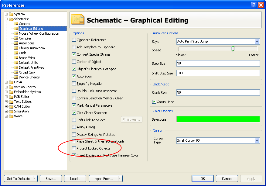
Enable the option to protect locked objects in the schematic.
Managing Footprints Across the Entire Design
Use the footprint manager to review and manage the footprints across the entire design.
Altium Designer's schematic editor includes a powerful Footprint Manager. Launched from the Schematic Editor's Tools menu (Tools » Footprint Manager), the Footprint Manager lets you review all the footprints associated with every component in the entire project. Multi-select support makes it easy to edit the footprint assignment for multiple components, change how the footprint is linked, or change the Current footprint assignment for components that have multiple footprints assigned. Design changes are applied through Altium Designer's standard ECO system, updating both the schematic and the PCB if required.
Using a Query to Find and Edit Multiple Objects
Altium Designer has a powerful query engine built into it, which is used to precisely target design objects. A query is essentially a description of something that you would like to find in the design data.
Filtering to Find the Objects
You can query the design data in a number of different ways. One of these is to type the query in to the Filter panel. When you apply the query you are filtering the design database. Each object is tested to see if complies with the query, and if it does, it is added to the result set.
The image below shows the Schematic Library SCHLIB Filter panel, with the query IsPin typed in. When this query is applied, every object in the library is checked (since the Whole Library option is enabled), any object that is a pin will comply and be added to the result set. All other objects are filtered out.
Using the SCHLIB Filter panel to query for Pins in the entire library in the Library Editor.
How the results are presented depends on the options on the right of the SCHLIB Filter panel. In the image above, you can see that objects that pass the filter (pins in this case) will be selected and zoomed. All other objects that do not pass the filter will be de-selected and masked out (faded and made non-editable).
Since the Select option is enabled, the pins will also be loaded into the SCH Inspector panel. This panel essentially 'stacks' the selected objects to give one view into their common properties, which is not that useful for editing component pins (unless perhaps you wanted to change their length).
The pins will also be displayed in the SCH List panel, which presents design data in a tabular grid, where it is easy to compare and edit one or more objects at once.
Editing Design Objects in the Schematic Library List Panel
Pins of the current component, presented in the SCHLIB List panel in the Schematic Library Editor.
The image above shows the Schematic Library SCHLIB List panel loaded with pins. Note that the from option at the top of the panel is currently set to current component, even though the filter was configured to select them for the whole library. There are scope controls in both the SCHLIB Filter and the SCHLIB List panels; this is because you control filtering separately from the display of the results. You can use this to do things like find all pins in the current library, then switch between looking at all the pins, or just those in the current component.
The tabular grid of the SCHLIB List panel is ideal for reviewing and editing objects. Once you have set the SCHLIB List panel to be in Edit mode (the option at the top left of the panel), you can use keys on the keyboard to 'walk' around and edit settings. For example, use the arrow keys to move around the grid, F2 or SPACEBAR to edit the selected cell, ENTER to apply a change, SPACEBAR to toggle a checkbox when that cell is active, and so on.
The SCHLIB List panel is completely configurable. To add or remove columns, or to change the order of columns, right-click on the column headings and select Choose Columns from the context menu.
Using a Spreadsheet Program to Edit Design Data
Not only can you edit data directly in the SCHLIB List panel, you can also multi-select blocks of cells and copy them from the SCHLIB List panel into your preferred spreadsheet program, and from the spreadsheet back into the SCHLIB List panel. For example, you are creating a new component and you have copied all the pin data from the manufacturer's datasheet into a spreadsheet.
Rather than entering this data into the Schematic Library editor one pin at a time, you can:
- Place one pin in the new schematic component, copy it, then use the Paste Array command to give you the total number of pins required.
- Use the query
IsPinin the Filter panel to load these pins into the List panel.
Pin data in the spreadsheet editor, as it is copied onto the clipboard
- Set up the relevant pin data columns, so that they correspond to the arrangement of columns in the spreadsheet program.
- Switch to the spreadsheet program, select the required block of pin data and copy it.
- Switch back to the SCHLIB List panel, select the same block of cells, right-click and select Paste from the context menu.
You might want to copy a block of data from the SCHLIB List panel to the spreadsheet first, to see how the data is represented in the spreadsheet. Using this approach, you can quickly configure a large number of component pins in your new component. The image above and the two below illustrate this sequence:.
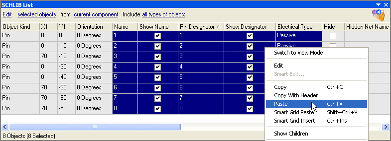
Select the target block of cells in the SCHLIB List panel, right-click and select Paste.

The SCHLIB List panel after the pin data has been pasted in
Creating and Editing Data as you Paste from a Spreadsheet or Table
You can also use the Smart Grid Paste tools to quickly update the design objects' attributes or to create a group of primitives quickly and easily. These tools are available via the right-click menu in the Schematic or PCB Editor's List panel.
For more information on using the Smart Grid Paste tools, refer to the Editing Attributes with Smart Grid Paste Tools section in SCH List page, or the Editing Attributes with Smart Grid Paste Tools section in the PCB List page.
the Altium Designer Panels Reference document.
Filtering Objects in the Design Workspace - How does it work?
Diagram of the filtering/highlighting process
The image above shows how design data is filtered and highlighted. Note how you can control the filtering process by writing a Query in the Filter panel, by configuring options in the Find Similar Objects (FSO) dialog (which actually uses a query behind the scenes), or by selecting objects in the Navigator panel. The PCB panel is not shown, however like the Navigator, it can also filter data in the PCB workspace.
The Highlighting engine determines how the filtered data will be presented.
As the user, you can access the filtered Display data in the main graphical editing window, in the Inspector (if you instructed the highlight engine to select the objects), or in the List panel.
Tips for Writing Queries
- Use the Query Helper to become familiar with the available query keywords. Click the Helper button in the Filter panel to display the helper.
- Press F1 over a keyword to display on-line help for that query keyword.
- Use the Mask field at the bottom of the Query Helper dialog to search for possible keywords. If you include the * wildcard character at the start of the string you are looking for, you will find all references to that text string in the keywords and also in the descriptions.
- Click the Check Syntax button before you close the Query Helper dialog.
- Include quotation marks around a variable, for example
'DIP14'. - There is an order of precedence used to resolve queries, so include brackets to be sure that it is resolved in the correct sequence.
For an overview of the query system read the Introduction to the Query Language, for detailed information on writing queries refer to the article, An Insiders Guide to the Query Language.