Tutorial - Getting Started with PCB Design
Contents
- The Design
- Creating a New PCB Project
- Adding a Schematic to the Project
- Setting Options
- Schematic Document Options
- Schematic Editor Preferences
- Locating the Components and Loading the Libraries
- Placing the Components on the Schematic
- Placing the Transistors
- Placing the Resistors
- Placing the Capacitors
- Installing the Connector Library
- Placing the Connector
- Component Positioning Tips
- Wiring up the Circuit
- Wiring Tips
- Nets and Net Labels
- Setting Up Project Options
- Checking the Electrical Properties of Your Schematic
- Setting up the Error Reporting
- Setting Up the Connection Matrix
- Setting up Class Generation
- Setting Up the Comparator
- Compiling the Project to Check for Errors
- Creating a New PCB
- Creating a New Board from a Template
- Configuring the Board Shape and Location
- Transferring the Design
- Ready to Start the PCB Design Process
- Setting Up the PCB Workspace
- Configuring the Display of Layers
- Creating a View Configuration
- Physical Layers and the Layer Stack Manager
- PCB Workspace Grids
- Imperial or Metric?
- Suitable Grid Settings
- Component Positioning and Placement options
- Setting Up the Design Rules
- Routing Width Design Rules
- Signal Nets Routing Width
- Power Nets Routing Width
- Defining the Electrical Clearance Constraint
- Defining the Routing Via Style
- Positioning the Components on the PCB
- Changing a Footprint
- Interactively Routing the Board
- Routing Tips
- Interactive Routing Modes
- Modifying and Rerouting
- Reroute an existing Route
- Re-arrange Existing Routes
- Track Dragging Tips
- Automatically Routing the Board
- Verifying Your Board Design
- Configuring the Display of Rule Violations
- Checking for Rule Violations
- Identifying the Error Conditions
- Viewing Your Board in 3D
- Tips for Working in 3D
- Output Documentation
- Available Output Types
- Generating Gerber Files
- Creating a Bill of Materials
Welcome to the world of electronic product development environment in Altium software. This tutorial will get you started by creating a simple PCB project based on an astable multivibrator design. If you are new to Altium software then it is worth reading the article The Altium Designer Environment, for an explanation of the interface, information on how to use panels, and managing design documents.
The Design
The design you will be capturing, and then designing a printed circuit board (PCB) for, is a simple astable multivibrator. The circuit is shown below, it uses two 2N3904 transistors configured as a self-running astable multivibrator.

Circuit for the multivibrator.
You are now ready to begin capturing (drawing) the schematic. The first step is to create a project.
Creating a New PCB Project
In Altium's software, a PCB project is the set of design documents (files) required to specify and manufacture a printed circuit board. The project file, for example MyProject.PrjPCB, is an ASCII text file that lists which documents are in the project, as well as other project-level settings, such as the required electrical rule checks, project preferences, and so on. Project outputs, such as print and CAM settings, can also be stored as project settings, or can also be defined in special-purpose OutputJob files, which give better control and visibility into the output process.
Source schematic sheets and the target output, for example the FPGA, embedded (VHDL), library package, or in this case the PCB design file, are then added to the project, with each one being referenced by a link inside the project file.
Once the source design is complete it can be compiled and design verification performed. When the source design is error free it can be transferred to the PCB workspace, using a process known as design synchronization. The next phase is to layout the PCB in accordance with the PCB design rules, the final phase is to generate the fabrication and assembly outputs.
The process of creating a new project is the same for all types of supported projects. This tutorial focuses on PCB design, so we will use the PCB project as an example. We will create the project file first and then create a blank schematic sheet to add the new empty project. Later in this tutorial we will create a PCB and add it to the project as well.
To start the tutorial, create a new PCB project:
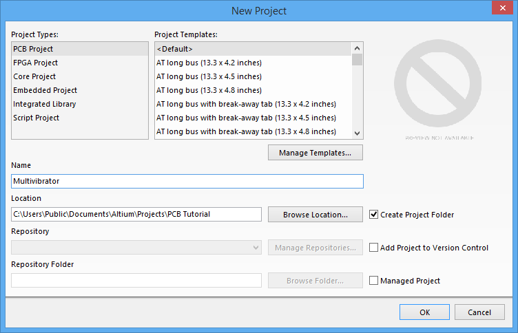
- Select File » New » Project from the menus, the New Project dialog will open.
- Note the list of available Project Types, confirm that
PCB Projectis selected. Ignore the Project Templates, these will not be used for this tutorial. - In the Name field, enter the name of the tutorial,
Multivibrator. There is no need to add the file extension, this will be added automatically. - In the Location field, type in a suitable location to save the project files, or click Browse to navigate to the required folder. Also enable the Create Project Folder option, this will create a sub-folder below the folder specified in the Location field, with the same name as the project.
Create the new project in the required location.
- Click OK to close the dialog and create the project file in the specified location.
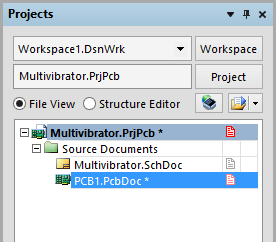
- The new project will appear in the Projects panel. If this panel is not displayed, click the System button at the bottom right of the main design window, and select Files from the menu that appears.
- The Projects panel will open, displaying the new project file, Multivibrator.PrjPCB, which will have no documents added.
Adding a Schematic to the Project
Next we will add a new schematic sheet to the project. It is on this schematic we will capture the astable multivibrator circuit.
Create a new schematic sheet by completing the following steps:
- Right-click on the project filename in the Projects panel, and select Add New to Project » Schematic. A blank schematic sheet named
Sheet1.SchDocwill open in the design window and an icon for this schematic will appear linked to the project in the Projects panel, under the Source Documents folder icon. - To save the new schematic sheet, select File » Save As. The Save As dialog will open, ready to save the schematic in the same location as the project file. Type the name Multivibrator in the File Name field and click Save. Note that files stored in the same folder as the project file itself (or in a child/grandchild folder) are linked to the project using relative referencing, whereas files stored in a different location are linked using absolute referencing.
- Since you have added a schematic to the project, the project file has changed too. Right-click on the project filename in the Projects panel, and select Save Project to save the project.
When the blank schematic sheet opens you will notice that the workspace changes. The main toolbar includes a range of new buttons, new toolbars are visible, the menu bar includes new items and the Sheet panel is displayed. You are now in the Schematic Editor. You can customize many aspects of the workspace. For example, you can reposition the panels and toolbars or customize the menu and toolbar commands.
Setting Options
Schematic Document Options
The first thing to do before you start drawing your circuit is to set up the appropriate document options. Complete the following steps.
- From the menus, choose Design » Document Options to open the Document Options dialog.
- For this tutorial, the only change we need to make here is to set the sheet size to A4, this is done in the Standard Styles field of the Sheet Options tab of the dialog.
- Confirm that both the Snap and Visible Grids are set to 10.
- Click OK to close the dialog and update the sheet size.
- To make the document fill the viewing area, select View » Fit Document (shortcut: V, D).
- Save the schematic by selecting File » Save (shortcut: F, S).
Schematic Editor Preferences
Next we will set the general schematic editor preferences.
- Select Tools » Schematic Preferences (shortcut: T, P) to open the schematic area of the Preferences dialog. This dialog allows you to set global preferences that will apply to all schematic sheets you work on.
- Open the Schematic - Default Primitives page of the dialog and enable the Permanent option (on the right hand side of the dialog). Click OK to close the dialog.
Locating the Components and Loading the Libraries
To manage the thousands of components and models that are available, the Schematic Editor includes powerful library searching capabilities. Although the components we require are in the default installed libraries, it is useful to know how to search through all libraries to find components. Work through the following steps to locate and add the libraries you will need for the tutorial circuit.
First we will search for the transistors, both of which are type 2N3904.
- If it is not visible, display the Libraries panel. The easiest way to do that is to click the System button down the bottom right of the software, then select Libraries from the menu that appears. Refer to the Working with Panels article to learn more about configuring and controlling panels.
- Press the Search button in the Libraries panel (or select Tools » Find Component) to open the Libraries Search dialog.
The Libraries Search dialogs can search across folders on the hard drive, or libraries already installed in the software.
- Ensure that the dialog options are set as follows:
- For the first Filter row, the Field is set to
Name, the Operator set tocontains, and the Value is3904. - The Scope is set to Search in
Components, and Libraries on path. - The Path is set to point to the installed Altium libraries, which will be something like
C:\Users\Public\Documents\Altium\AD15\Library.
- For the first Filter row, the Field is set to
- Click the Search button to begin the search. The Query Results are displayed in the Libraries panel as the search takes place - there should be one component found, as shown in the image below.
- You can only place components from Libraries that are installed in the software, if you attempt to place from a library that is not currently installed you will be asked to Confirm the installation of that library when you attempt to place the component. Alternatively, install the library by right-clicking on the found component and selecting Install Current Library, as shown in the image above.
- Since the Miscellaneous Devices library is already installed, the component is ready to place. Added libraries appear in the drop down list at the top of the Libraries panel, as you select a library in the list the components in that library are listed below. Select the Miscellaneous Devices library from the list, then use the component Filter in the panel to locate the required
2N3904component within the library. - Click on the component name
2N3904to select it. The Models region of the panel shows that this component has a footprint, a simulation model and a signal integrity model.
Filtering the library for components with the string 3904 in their name.
Placing the Components on the Schematic
The first components we will place on the schematic are the two transistors, Q1 and Q2. Refer to the rough schematic sketch shown above for the general layout of the circuit.
Placing the Transistors
- Select View » Fit Document (shortcut: V, D) to ensure your schematic sheet takes up the full window.
- Using the techniques just described, locate and display the
2N3904device in the Libraries panel. - Click on the 2N3904 entry in the list to select it, then click the Place button. Alternatively, double-click on the component name, or click and drag it into the workspace. The cursor will change to a cross hair and you will have an outlined version of the transistor floating on your cursor. You are now in part placement mode. If you move the cursor around, the transistor outline will move with it.
Do not place the transistor yet!
- Before placing the part on the schematic, we will edit its properties - which can be done for any object floating on the cursor. While the transistor is still floating on the cursor, press the Tab key to open the Component Properties dialog. We will now set up the dialog options to appear as below.
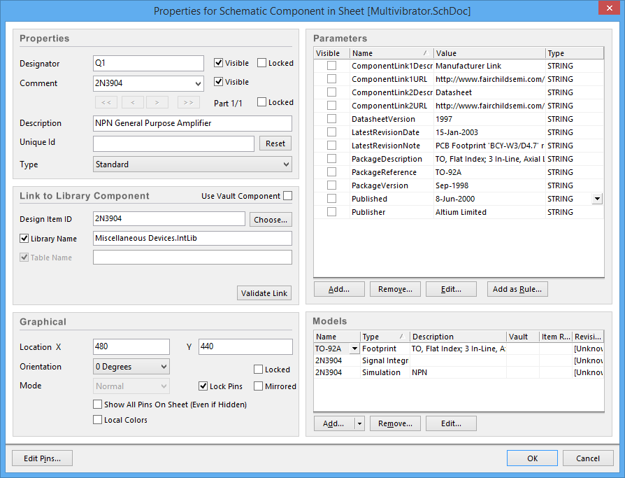
Set the Designator to Q1, and confirm that the Footprint is TO-92A.
- In the Properties section of the dialog, type in the Designator
Q1. - Confirm that the Footprint (specified in the Models region of the dialog) is set to TO-92A. Since this is an integrated library each component has a symbol and at least 1 footprint, as well as simulation models for some of the components.
- Leave all other fields at their default values, and click OK to close the dialog.
- Move the cursor, with the transistor symbol attached, to position the transistor a little to the left of the middle of the sheet. Note the current snap grid, it is displayed on the left of the Status bar down the bottom of the application. It defaults to 10, you can press the G shortcut to cycle through the available grid settings during placement. It is strongly advised to keep the snap grid at 10 or 5, to keep the circuit neat, and make it easy to attach wires to pins.
- Once you are happy with the transistor's position, left mouse click or press Enter on the keyboard to place the transistor onto the schematic.
- Move the cursor and you will find that a copy of the transistor has been placed on the schematic sheet, but you are still in part placement mode with the part outline floating on the cursor. This feature allows you to place multiple parts of the same type. So let's now place the second transistor. This transistor is the same as the previous one, so there is no need to edit its attributes before we place it. The software will automatically increment a component's designator when you place a series of parts. In this case, the next transistor we place will automatically be designated Q2.
- If you refer to the rough schematic diagram shown before, you will notice that Q2 is drawn as a mirror of Q1. To flip the orientation of the transistor that is floating on the cursor, press the X key on the keyboard. This flips the component horizontally (along the X axis).
- Move the cursor to position the part to the right of Q1. To position the component more accurately, press the PageUp key twice to zoom in two steps. You should now be able to see the grid lines.
- Once you have positioned the part, left mouse click or press Enter to place Q2. Once again a copy of the transistor you are "holding" will be placed on the schematic, and the next transistor will be floating on the cursor ready to be placed.
- Since we have now placed all the transistors, we will exit part placement mode by clicking the Right Mouse Button or pressing the ESC key. The cursor will revert back to a standard arrow.
The placed transistors.
- In the Libraries panel, make sure the Miscellaneous Devices.IntLib library is active.
- Set the filter by typing
resin the filter field below the Library name. - Click on
Res1in the components list to select it, then click the Place button. You will now have a resistor symbol floating on the cursor. - Press the Tab key to open the Component Properties dialog to edit the resistor's attributes.
- In the Properties section of the dialog, configure the designator by typing
R1in the Designator field. - The contents of Comment field of the schematic component maps to the Comment field of the PCB component, typically you would enter the value or the resistor here. Alternatively, you can map any of the component parameters into the Comment field, to do this type
=Valueinto the Comment field for R1, and enter a value of100kinto the Value parameter. Configuring and using the Value parameter means you can also perform a circuit simulation with this design. - Because you are mapping the Value parameter into the Comment you do not need to display the Value parameter as well, so ensure that the Visible option for the Value parameter is disabled.
- Make sure that footprint name AXIAL-0.3 is the current footprint in the Models list.

Enter the Designator and Value, and map the Value into the Comment field, so that it transfers to the PCB.
- Click OK to close the Component Properties dialog, the resistor will be floating on the cursor.
- Press the Spacebar to rotate the resistor by 90° so it is in the correct orientation.
- Position the resistor above the base of Q1 (refer to the schematic diagram shown earlier) and click the Left Mouse Button or press Enter to place the part. Don't worry about making the resistor connect to the transistor just yet. We will wire up all the parts later.
- Next place the other 100k resistor, R2, above the base of Q2. The designator will automatically increment when you place the second resistor.
- The remaining two resistors, R3 and R4, have a value of 1K, so press the Tab key to open the Component Properties dialog, enter
1kinto the Value parameter. Click OK to close the dialog. - Position and place R3 and R4 as shown in the image below.
- Right-click or press ESC to exit part placement mode.
The circuit with the transistors and resistors placed.
Placing the Capacitors
Now place the two capacitors.
- The capacitor part is also in the Miscellaneous Devices.IntLib library, which should already be selected in the Libraries panel.
- Type
capin the component's filter field in the Libraries panel. - Click on CAP in the components list to select it, then click the Place button. You will now have a capacitor symbol floating on the cursor.
- Press the Tab key to edit the capacitor's attributes. In the Component Properties dialog set the Designator to
C1, the Comment to=Value, set the Value parameter to20n,disable the Visible option for the Value parameter, and check the PCB footprint model RAD-0.3 is selected in the Models list. Click OK. - Using the image below as a guide, position and place the two capacitors in the same way that you placed the previous parts.
- Right-click or press Esc to exit placement mode.
Circuit with the capacitors also placed.
Installing the Connector Library
The last component to be placed is the connector, located in Miscellaneous Connectors.IntLib. This integrated library is normally already installed, if it is not:
- Click the Libraries button at the top of the Libraries panel, the Available Libraries dialog will open. This dialog lists all libraries that are currently available to place parts from, separated into 3 categories:
- Project libraries - libraries that have been added to the project, which are automatically made available when that project is the active project.
- Installed libraries - libraries that you as the designer have installed, this list is stored for this installation of the software.
- Search Path - paths defined on this tab are searched for suitable library types, and detected components and models are then made available. Typically used for simulation models, not recommended for schematic and PCB components/models as all folders / files are searched.
- On the Installed tab of the Available Libraries dialog, click the Install button and select Install from File.
- The Open dialog will appear, locate and Open the Miscellaneous Connectors.IntLib (typically in
C:\Users\Public\Documents\Altium\AD15\Library\). - Close the Available Libraries dialog.
Placing the Connector
Once the Miscellaneous Connectors.IntLib has been installed:
- Select Miscellaneous Connectors.IntLib from the Libraries list in the Libraries panel. The connector we want is a two-pin socket, so type
*2into the Libraries panel filter field. - Select
Header 2from the parts list and click the Place button. Press Tab to edit the attributes and set Designator toY1and check that the PCB footprint model is HDR1X2. No Value parameter is required as you would replace this component with a power source when simulating the circuit. Click OK to close the dialog. - Before placing the connector, press X to flip it horizontally so that it is in the correct orientation. Click to place the connector on the schematic, as shown in the image below.
- Right-click or press ESC to exit part placement mode.
- Save your schematic by selecting File » Save from the menus (shortcut: F, S).
Circuit with all parts placed.
You have now placed all the components. Note that the components shown in the figure below are spaced so that there is plenty of room to wire to each component pin. This is important because you can not place a wire across the bottom of a pin to get to a pin beyond it. If you do, both pins will connect to the wire. If you need to move a component, click-and-hold on the body of the component, then drag the mouse to reposition it.
Component Positioning Tips
- To reposition any object, place the cursor directly over the object, click-and-hold the left mouse button, drag the object to a new position and then release the mouse button. Movement is constrained to the current snap grid, which is displayed on the Status bar, press the G shortcut at any time to cycle through the current snap grid settings. Remember that it is important to position components on a coarse grid, such as 5 or 10.
- You can also re-position a group of selected schematic objects using the arrow keys on the keyboard. Select the objects, then press an arrow key while holding down the Ctrl key. Hold Shift as well to move objects by 10 times the current snap grid.
- The grid can also be temporarily set to 1 while moving an object with the mouse, hold Ctrl to do this. Use this feature when positioning text.
- The grids you cycle through when you press the G shortcut are defined in the Schematic - Grids page of the Preferences dialog (DXP » Preferences). The Schematic - Default Units page of the Preferences dialog is used to select the type of units that will be used, select between DXP Defaults, Imperial, or Metric. Note that Altium components are designed using the DXP Defaults grid, if you change to a metric grid the component pins will no longer fall onto a grid of 10.
Wiring up the Circuit
Wiring is the process of creating connectivity between the various components of your circuit. To wire up your schematic, refer to the sketch of the circuit, or the animation shown below, and complete the following steps:
- To make sure you have a good view of the schematic sheet, press the PageUp key to zoom in or PageDown to zoom out. Alternatively, hold down the Ctrl key and roll the mouse wheel to zoom in/out, or hold Ctrl + Right Mouse button down and drag the mouse up/down to zoom in/out.
- Firstly wire the lower pin of resistor R1 to the base of transistor Q1 in the following manner. Select Place » Wire (shortcut: P, W) from the menus or click on the Wire tool from the Wiring toolbar to enter the wire placement mode. The cursor will change to a crosshair.
- Position the cursor over the bottom end of R1. When you are in the right position, a red connection marker (large cross) will appear at the cursor location. This indicates that the cursor is over a valid electrical connection point on the component.
- Click the Left Mouse Button or press Enter to anchor the first wire point. Move the cursor and you will see a wire extend from the cursor position back to the anchor point. The default corner mode is a right angle, the tip box below explains how to change the corner mode, for this circuit right angle is the best choice.
- Position the cursor over the base of Q1 until you see the cursor change to a red connection marker. Click or press Enter to connect the wire to the base of Q1. The cursor will release from that wire.
- Note that the cursor remains a cross hair, indicating that you are ready to place another wire. To exit placement mode completely and go back to the arrow cursor, you would Right-Click or press ESC again - but don't do this just now.
- We will now wire C1 to Q1 and R1. Position the cursor over the left connection point of C1 and click or press Enter to start a new wire. Move the cursor horizontally till it is directly over the wire connecting the base of Q1 to R1, and click or press Enter to place the wire segment. Again the cursor will release from that wire, and you remain in wiring mode, ready to place another wire. Note how a junction automatically appears to connect the two wires.
- Wire up the rest of your circuit, as shown in the figure below.
- When you have finished placing all the wires, right-click or press ESC to exit placement mode. The cursor will revert to an arrow.
A simple animation showing the schematic being wired.
Wiring Tips
- Left-click or press Enter to anchor the wire at the cursor position.
- Press Backspace to remove the last anchor point.
- Press Spacebar to toggle the direction of the corner. You can observe this in the animation shown above, when the connector is wired.
- Press Shift+Spacebar to cycle through all possible corner modes. The right-angle mode is the most suitable for this design.
- Right-click or press Esc to exit wire placement mode.
- To graphically edit the shape of a wire, Click once to select it first, then Click and hold on a segment or vertex to move it.
- Whenever a wire crosses the connection point of a component, or is terminated on another wire, a junction will automatically be created.
- A wire that crosses the end of a pin will connect to that pin, even if you delete the junction. Check that your wired circuit looks like the figure shown, before proceeding.
- To move a placed component and drag connected wires with it, hold down the Ctrl key while moving the component, or select Move » Drag.
An animation showing dragging - hold Ctrl as you click and drag to maintain connectivity.
Nets and Net Labels
Each set of component pins that you have connected to each other now form what is referred to as a net. For example, one net includes the base of Q1, one pin of R1 and one pin of C1. Each net is automatically assigned a system-generated name, which is based on one of the component pins in that net.
To make it easy to identify important nets in the design, you can add Net Labels to assign your preferred name. To place net labels on the two power nets:
- Select Place » Net Label (shortcut: P, N). A net label will appear floating on the cursor.
- To edit the net label before it is placed, press Tab key to open the Net Label dialog.
- Type
12Vin the Net field, then click OK to close the dialog. - Place the net label so that the bottom left corner of the net label touches the upper most wire on the schematic, as shown in the image below. The cursor will change to a red cross when the net label is correctly positioned to connect to the wire. If the cross is light grey, it means there will not be a valid connection made.
The net label in free space (left image) and positioned over a wire (right image), note the red cross.
- After placing the first net label you will still be in net label placement mode, so press the Tab key again to edit the second net label before placing it.
- Type
GNDin the Net field and click OK to close the dialog. - Place the net label so that the bottom left of the net label touches the lower most wire on the schematic (as shown in the image below). Right-click or press ESC to exit net label placement mode.
- Select File » Save (shortcut: F, S) to save your circuit. Save the project as well.
The completed schematic, ready to check for errors.
Congratulations! You have just completed your first schematic capture. Before we turn the schematic into a circuit board we need to configure the project options, and check the design for errors.
Setting Up Project Options
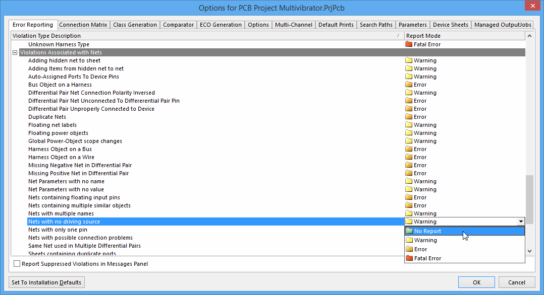
Configure the Error Reporting tab to detect for design errors.
All project-specific settings are configured in the Options for Project dialog (Project » Project Options). The project options include the error checking parameters, a connectivity matrix, Class Generator, the Comparator setup, ECO generation, output paths and netlist options, Multi-Channel naming formats, Default Print setups, Search Paths, Project level Parameters, Device Sheet settings and Settings for Managed Output Jobs. These settings are used when you compile the project.
Project outputs, such as assembly, fabrication outputs and reports can be set up from the File and Reports menus. These settings are also stored in the Project file so they are always available for this project. Alternatively you can set up output options in an Output Job file (File » New » Output Job File). See Documentation Outputs for more information.
Checking the Electrical Properties of Your Schematic
Schematic diagrams are more than just simple drawings - they contain electrical connectivity information about the circuit. You can use this connectivity awareness to verify your design. When you compile a project, the software checks for errors according to the rules set up in the Error Reporting and Connection Matrix tabs of the Options for Project dialog. When you compile the project any violations that are detected will display in the Messages panel.
- Select Project » Project Options to open the Options for Project dialog (shown in the image above).
- Set up any project-related options in this dialog. We will now make some changes to the Error Reporting, Connection Matrix and Comparator tabs.
Setting up the Error Reporting
The Error Reporting tab in the Options for Project dialog is used to set up design drafting checks. The Report Mode settings show the level of severity of a violation. If you wish to change a setting, click on a Report Mode next to the violation you wish to change and choose the level of severity from the drop-down list. For this tutorial we will use the default settings in this tab.
Setting Up the Connection Matrix
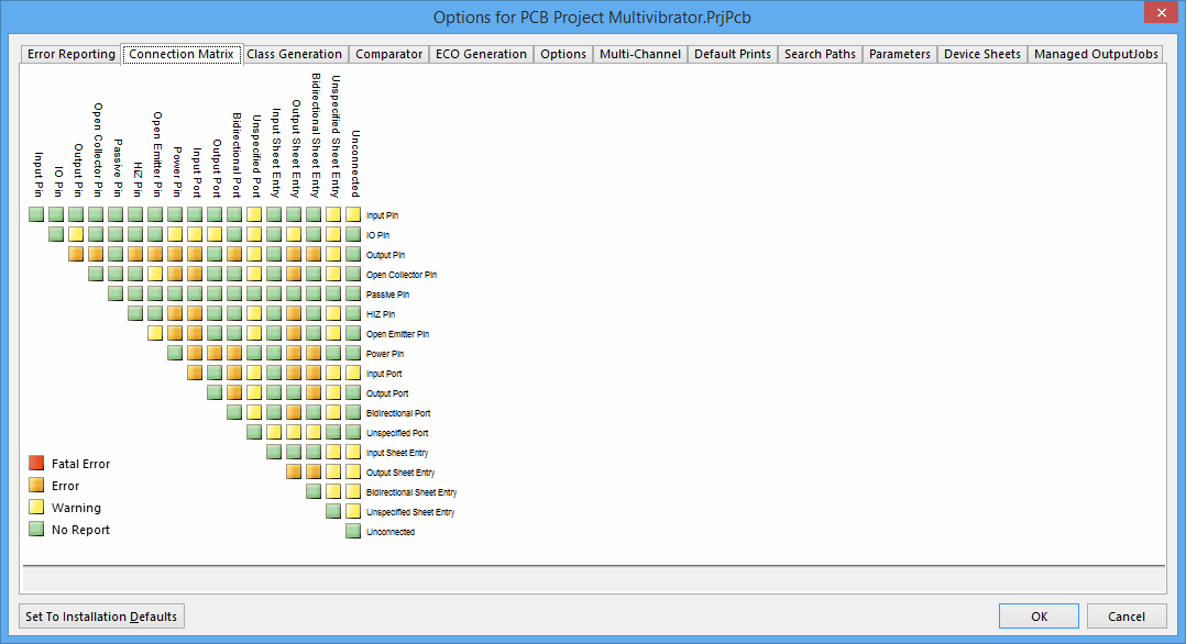
The Connection Matrix defines what electrical conditions are checked for on the schematic.
When the design is compiled a list of the pins in each net is built in memory. The type of each pin is detected (eg: input, output, passive, etc), and then each net is checked to see if there are pin types that should not be connected to each other, for example an output pin connected to another output pin. The Connection Matrix tab of the Options for Project dialog is where you configure what pin types are allowed to connect to each other. For example, look down the entries on the right side of the matrix diagram and find Output Pin. Read across this row of the matrix till you get to the Open Collector Pin column. The square where they intersect is orange, indicating that an Output Pin connected to an Open Collector Pin on your schematic will generate an error condition when the project is compiled.
You can set each error type with a separate error level, eg. from no report, through to a fatal error. To make changes to the Connection Matrix:
- To change one of the settings click the colored box, it will cycle through the 4 possible settings. Note that you can right-click on the dialog face to display a menu that lets you toggle all settings simultaneously, including an option to restore them all to their Default state (handy if you have been toggling settings and cannot remember their default state).
- Our circuit contains only Passive Pins (on resistors, capacitors and the connector) and Input Pins (on the transistors). Let's check to see if the connection matrix will detect unconnected passive pins. Look down the row labels to find Passive Pin. Look across the column labels to find Unconnected. The square where these entries intersect indicates the error condition when a passive pin is found to be unconnected in the schematic. The default setting is green, indicating that no report will be generated.
- Click on this intersection box until it turns Orange, so that an error will be generated for unconnected passive pins when we compile the project. We will purposely create an instance of this error to check it later in this tutorial.
Setting up Class Generation

Component and net classes can be generated from the schematic, as well as placement rooms.
When the design is transferred to the PCB, component classes, net classes, and placement rooms can be generated automatically. This is particularly useful for a well-structured hierarchical design, creating a component class and component placement room from each sheet, and a net class from each bus. This default behavior is not necessary for this simple design, to disable this:
- Click the Class Generation tab, and disable the Component Classes check box, as shown in the image above. Doing this automatically disables the Generate Rooms option as well.
Setting Up the Comparator

The Comparator tab is used to configure exactly what differences the comparison engine will check for.
The Comparator tab in the Options for Project dialog sets which differences between files will be reported or ignored when a project is compiled. Generally the only time you will need to change settings in this tab is when you add extra detail to the PCB, such as net classes or rooms, and do not want those settings removed. If you need more detailed control, then you can selectively control the comparator using the individual comparison settings. Settings that are often changed in this tab for more complex designs include: Extra Component Classes and Extra Net Classes.
- For this tutorial it is sufficient to confirm that the Ignore Rules Defined in PCB Only option is enabled.
We are now ready to compile the project and check for any errors.
Compiling the Project to Check for Errors
Compiling a project checks for drafting and electrical rules errors in the design documents and details all warnings and errors in the Messages panel, and also gives detailed information in the Compiled Errors panel. We have already set up the rules in the Error Checking and Connection Matrix tabs of the Options for Project dialog, so we are ready to check the design.
- To compile the Multivibrator project, select Project » Compile PCB Project Multivibrator.PrjPcb. If you have already compiled, select Project » Recompile PCB Project Multivibrator.PrjPcb.
- When the project is compiled, all warnings and errors are displayed in the Messages panel. The panel will only appear automatically if there are errors detected, to open it manually click the System button down the bottom right of the workspace, and select Messages from the menu.
- If your circuit is drawn correctly, the Messages panel should not contain any errors, just the message Compile successful, no errors found. If the there are errors, work through each one, checking your circuit and ensuring that all wiring and connections are correct.
We will now deliberately introduce an error into the circuit and recompile the project:
- Click on the Multivibrator.SchDoc tab at the top of the design window to make the schematic sheet the active document.
- Click in the middle of the wire that connects R1 to the base wire of Q1. Small, square editing handles will appear at each end of the wire and the selection color will display as a dotted line along the wire to indicate that it is selected. Press the Delete key on the keyboard to delete the wire.
- Recompile the project (Project » Recompile PCB Project Multivibrator.PrjPcb) to check for errors. The Messages panel will display warning messages indicating you have unconnected pins in your circuit.
- The Messages panel is divided horizontally into 2 regions, as shown in the image below. The upper region lists all messages; which can be saved, copied, cross probed to or cleared via the right-click menu. The lower region details the warning/error currently selected in the upper region of the panel.
- When you double-click on an error or warning in either region of the Messages panel, the schematic view will pan and zoom to the object in error.
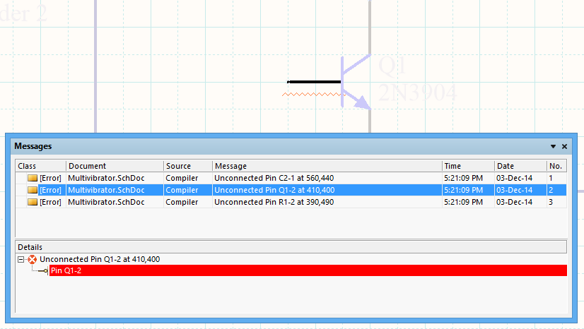
Use the Messages panel to locate and resolve design errors - double-click on an error to pan and zoom to that object.
Before we finish this section of the tutorial, let's fix the error in our schematic.
- Make the schematic sheet the active document.
- Either select Edit » Undo from the menus (shortcut: Ctrl + Z) to restore the deleted wire, or re-place the wire (Place » Wire).
- To check that there are no errors, recompile the project (Project » Compile PCB Project Multivibrator.PrjPcb) - the Messages panel should show no errors.
- Select View » Fit All Objects (shortcut: V, F) from the menus to display the entire schematic.
- Save the schematic and the project file as well.
Schematic capture is now complete, time to create the PCB!
Creating a New PCB
Main article: Preparing the Board for Design Transfer
Before you transfer the design from the Schematic Editor to the PCB Editor, you need to create the blank PCB with at least a board outline. There are a number of ways of creating the blank board, including:
- Importing a DXF file that includes objects that define the shape. These can then be selected, and the board shape defined from selected objects.
- Placing a STEP object that includes the board definition.
- Creating a new, empty PCB and redefining the board shape.
- Using a template board, and then adjusting the board shape.
For this tutorial, the last approach will be used.
Creating a New Board from a Template
To create a new PCB, based on a template:
- Display the Files panel. The default location for this panel is docked on the left side of the software. If the Files panel is not available, click the System button down the bottom right of the workspace and select Files from the menu that appears.
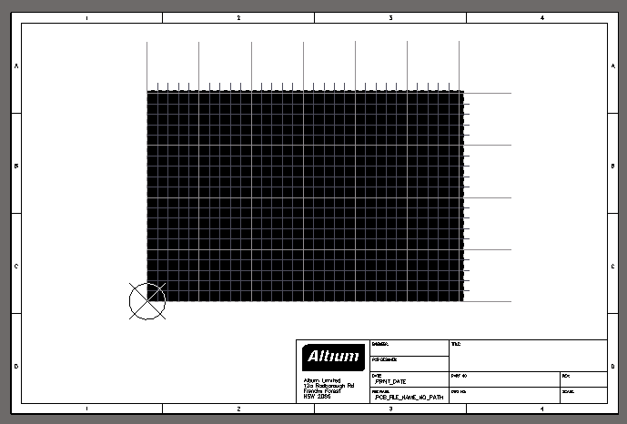
- In the New from template section, click the PCB Templates link to open the Choose Existing Document dialog. This dialog opens to display the contents of the
\Templatesfolder included in the software installation. - Locate and select the
A4.PcbDoctemplate. When you click to select it, the board will immediately open. An HTM document might also open, informing you that the file was generated in an earlier version of the software. These warning documents are important, as they often detail any changes that might affect the design rule checking process. In this case, for a new blank board, you can simply close the document (right-click on the document tab at the top and select Close A4.PCBDOC.htm). - Your screen will display what looks like a white sheet with boarder markers and a title block, with a black region in it. The black region is the board shape, that is what gets fabricated and assembled. Note that the A4 size refers to the overall document size, not the board size.
![]()
The new blank board, ready to be resized and configured.
Configuring the Board Shape and Location
There are a number of attributes of this blank board that need to be changed before transferring the design from the schematic editor, including:
- Changing from imperial to metric units
- Setting the board origin
- Selecting a suitable snap grid
- Redefining the board shape to the required size
- Configuring the layers used in the design
- The current workspace units are displayed on the Status bar, displayed along the bottom of the software. To change the units, press Q on the keyboard to toggle between Imperial and Metric units, for this tutorial metric units will be used.
- There are two origins used in the software, the Absolute Origin, which is the lower left of the workspace, and the user-definable Relative Origin, which is used to determine the current workspace location. Before setting the origin, zoom in to the lower left of the current board shape until you can easily see the grid - to do this position the cursor over the lower-left corner of the board shape and press PageUp until both the Coarse and Fine grids are visible, as shown in the images below.
- To set the Relative Origin, select Edit » Origin » Set, position the cursor over the bottom left corner of the board shape, then left click to locate it.
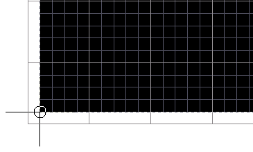
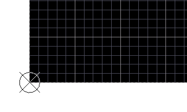
Select the command, position the cursor over the corner of the board (left image), then click to define the origin (right image).
- The next step is to select a suitable snap grid. You may have noticed that the current snap grid is 0.127mm, which is the old 10mil imperial snap grid converted to metric. To change the snap grid at any time, press Ctrl+G to open the Cartesian Grid Editor. Since you are about to define the overall size of the board a very coarse grid can be used, type
5mminto the Step X field in the dialog and click OK. Grids are discussed in more details later in the tutorial. - To zoom back out and show the all of the workspace currently being used, press V, D (View » Document). Your design should look much like the image shown below.
- The PCB editor can display the design in 3 different modes, Board Planning Mode (1), 2D Layout Mode (2) and 3D Layout Mode (3). You can switch modes using the shortcuts just detailed, or select the required mode in the View menu. Switch to Board Planning Mode, your board should now look like the image shown on the right below.
Switch from 2D to Board Planning Mode so you can redefine the board shape.
- Your choice now is to either redefine the board shape (draw it again), or edit the existing board shape. For a simple square or rectangle, it is more efficient to edit the existing board shape, to do this select Design » Edit Board Shape. Editing handles will appear at each corner and the center of each edge.
- The objective is to resize the shape to create a 50mm by 50mm board. The Coarse visible grid is 25mm (5x the snap grid), this will be used as a guide. You can now either: slide the upper and right edges down and in to create the correct size; or move 3 of the corners in, leaving the one that is at the origin in its current location. To slide the top edge down, position the cursor over the edge (but not over a handle), click and hold, then drag the edge to the new location (so the board height is 2 of the coarse grid lines). Repeat the process to move the right-hand edge in.
- The last step is to reposition the board shape (Design » Move Board Shape), positioning it be approximately in the middle of the A4 page. After you have moved it, you will need to reset the origin to the bottom left of the board.
Resizing the board shape to the required size (note the editing cursor in the left image), then move the shape to the center of the page.
- Before transferring the design from the schematic editor, you need to make the board part of the project and save it. To make it part of the project, click and hold on the
PCB1.PcbDocicon in the Projects panel, then drag and drop it onto the project, as shown in the images below.

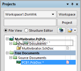
Drag and drop the PCB file onto the project file to make it part of the project. The reverse process can be used to remove a file from the project.
- Switch the PCB editor back to 2D Layout Mode, and save the PCB into the same folder as the project and schematic, with the name
Multivibrator.PcbDoc. Adding the board file to the project means the project has also been modifed, right-click on the project in the Projects panel and save it.
Transferring the Design
The process of transferring a design from the capture stage to the board layout stage is launched by selecting Design » Update PCB Document Multivibrator.PcbDoc from the Schematic Editor menus, or Design » Import Changes from Multivibrator.PcbDoc from the PCB Editor menus - when you do the design is compiled and a set of Engineering Change Orders is created, that will perform the following steps:
- A list of all components used in the design is built, and the footprint required for each. When the ECOs are executed the software will attempt to locate each footprint in the currently available libraries, and place each into the PCB workspace. If the footprint is not available, an error will occur.
- A list of all nets (connected component pins) in the design is created. When the ECOs are executed the software will add each net to the PCB, and then attempt to add the pins that belong to each net. If a pin cannot be added an error will occur - this happens when the footprint was not found, or the pads on the footprint do not map to the pins on the symbol.
- Addition design data is then transferred, including placement rooms, net and component classes, and PCB design rules.
You are now ready to transfer the design from schematic capture to PCB layout. To transfer the schematic information to the target PCB:
- Open the schematic document, Multivibrator.SchDoc.
-
Select Design » Update PCB Document (Multivibrator.PcbDoc). The project will compile and the Engineering Change Order dialog open.
An ECO is created for each change that needs to be made to the PCB so that it matches the schematic.
- Click on Validate Changes. If all changes are validated, a green tick will appear next to each change in the Status list. If the changes are not validated, close the dialog, check the Messages panel and resolve any errors.
- Click on Execute Changes to send the changes to the PCB. When completed, the Done column entries become ticked (as shown in the image above).
- The target PCB opens with the Engineering Change Order dialog open on top of it, click to Close the dialog.
- The components will have been positioned outside of the board, ready for placing on the board. Use the shortcut V, D (View » Document) if you cannot see the components in your current view.
Ready to Start the PCB Design Process
Once all of the ECOs have been executed the components and nets will appear in the PCB workspace, just to the right of the board outline.
Note that the PCB Editor is capable of rendering the PCB design in both 2 Dimensional and 3 Dimensional modes. 2D mode is a multi-layered environment that is ideal for normal PCB design tasks, such as placing and routing the components. 3D mode is useful for examining your design both inside and out as a full 3D model. Note that 3D mode does not provide the same range of functionality available in 2D mode. You can switch between 2D and 3D modes through View » 2D Layout Mode or View » 3D Layout Mode (shortcuts: 2 (2D), 3 (3D)).
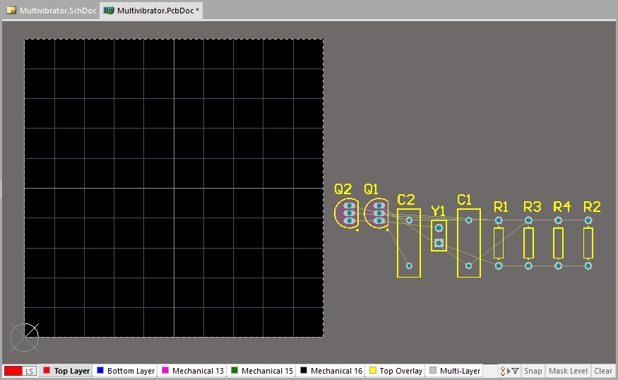
The components and nets needed for the design, placed in the PCB workspace (configuring this display is described below).
Setting Up the PCB Workspace
Main article: Preparing the Board for Design Transfer
Before we start positioning the components on the board we need to configure certain PCB workspace and board settings, such as the layers, grids and design rules.
Configuring the Display of Layers
As well as the the layers used to fabricate the board, including: signal, power plane, mask and silkscreen layers, the PCB Editor also supports numerous other non-electrical layers. The layers are often grouped in the following way:
- Electrical layers - includes the 32 signal layers and 16 internal power plane layers.
- Mechanical layers - there are 32 general purpose mechanical layers, used for design tasks such as dimensions, fabrication details, assembly instructions, or special purpose tasks such as glue dot layers. These layers can be selectively included in print and Gerber output generation. They can also be paired, meaning that objects placed on one of the paired layers in the library editor, will flip to the other layer in the pair when the component is flipped to the bottom side of the board.
- Special layers - these include the top and bottom silkscreen layers, the solder and paste mask layers, drill layers, the Keep-Out layer (used to define the electrical boundaries), the multilayer (used for multilayer pads and vias), the connection layer, DRC error layer, grid layers, hole layers, and other display-type layers.
The display attributes of all layers are configured in the View Configurations dialog (Design » Board Layers and Colors, or press the L shortcut).
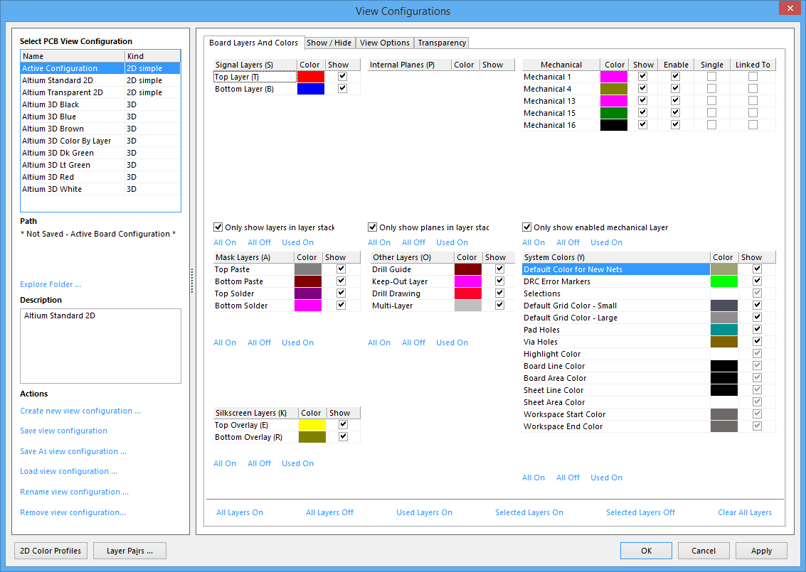
Press the L shortcut to open the View Configurations dialog.
As well as the layer display state and color settings, the View Configurations dialog also gives access to other display settings, including:
- How each type of object is displayed (solid, draft or hidden), in the Show/Hide tab of the dialog.
- Various view options, such as if Pad Net names and Pad Numbers are to be displayed, the Origin Marker, if Special Strings should be converted, and so on. These are configured in the View Options tab of the dialog.
- Switch to the View Options tab.
- Confirm that the Show Pad Nets option is enabled, and the Net Names on Tracks Display is set to
Single and Centered. - Click OK to accept the settings and close the dialog.
Creating a View Configuration
Since there are so many layers, and since during the design process you will work with many different settings of layers turned on and off, the current settings in the View Configurations dialog can be saved as a View Configuration. You can easily switch between available View Configurations via the menu in the main toolbar, as shown below.
Use the dropdown to quickly switch between view configurations.
View configurations are settings that control numerous PCB workspace display options for both 2D and 3D display modes (and apply to both the PCB and PCB Library Editors). The view configuration last used when saving a PCB document is also saved with the file itself. This enables it to be viewed on another instance of the software, using that same view configuration. View configurations can also be saved locally and be used and applied at any time to any PCB document. If you open a PCB file that does not have an associated view configuration, a system default one is used. View Configurations are created and saved using the options on the left hand side of the View Configurations dialog.
Let's create a simple 2D view configuration for this tutorial.
- Press L to open the View Configurations dialog (Design » Board Layers & Colors). The dialog opens with the active configuration selected in the Select PCB View Configuration area on the top left. If you were in 3D mode, click on a 2D configuration.
- In the Board Layers And Colors tab, ensure that the Only show layers in layer stack and Only show enabled mechanical layers options are enabled. These settings will display only the layers in the stack.
- Click the Used Layers On control at the bottom of the page. This will display only layers that are currently being used, that is, the layers that have design objects on them.
- If required, disable the display of the four Mask layers, the Drill Guide and Drill Drawing layers.
- In the Mechanical Layers section, enable the Linked To checkbox for Mechanical 16. The reason for this is that this is the layer the sheet boarder and title block have been drawn on, if you link this layer to the sheet then when you hide the white sheet, that layer is also hidden.
- In the Actions section, click Save As view configuration and save the file as
Tutorialin the default location. Note that you do not need to type in the file extension, this is always added automatically. - Click OK when you return to the View Configurations dialog to apply the changes and close it.
- Your new View Configuration will now be active, you can confirm this by checking in the drop down View Configuration list in the main toolbar (as shown in the image above.
- The last step is to hide the white background sheet, as it makes it difficult to see the component silkscreen. To turn it off press D, O to open the Board Options dialog, where you can clear the Display Sheet checkbox.
Physical Layers and the Layer Stack Manager
Main article: PCB Layer Stack Management
The PCB Editor supports up to 32 signal and 16 power plane (solid copper) layers, as well as the the soldermask and silkscreen layers. The arrangement of these layers is referred to as the Layer Stack.
The tutorial PCB is a simple design and can be routed as a single-sided or double-sided board.
To examine and configure the layer stack for your board:
- Open the Layer Stack Manager, to do this select Design » Layer Stack Manager (D, K). For a new board, its single default stack comprises: a dielectric core, 2 copper layers, as well as the top and bottom soldermask (coverlay) and overlay (silkscreen) layers, as shown in the image below.
- New layers and planes are added below the currently selected layer, which is done via the Add Layer button, or the right-click menu.
- Layer properties, such as material, copper thickness and dielectric properties, are included when a Layer Stack Table is placed, and are also used for signal integrity analysis. Double-click in a cell to configure that setting. For example, the Thickness settings shown in the image below have been changed slightly to more suitable metric values.
- When you have finished exploring the layer stack options, restore the values to those shown in the image below and click OK to close the dialog.
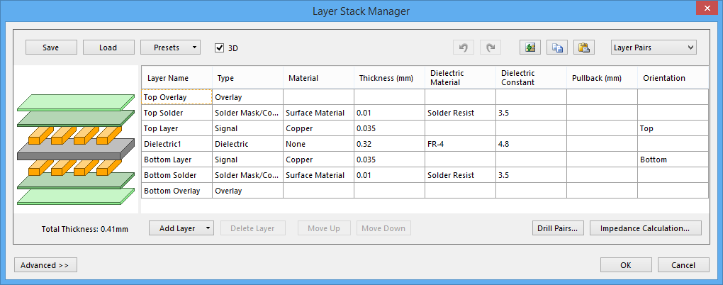
The properties of the physical layers are defined in the Layer Stack Manager.
PCB Workspace Grids
The next step is to select a grid that is suitable placing and routing the components. All the objects placed in the PCB workspace are placed on the current snap grid.
Imperial or Metric?
Traditionally, the grid was selected to suit the component pin pitch and the routing technology that you planned to use for the board - that is, how wide do the tracks need to be, and what clearance is needed between tracks. The basic idea is to have both the tracks and clearances as wide as possible, to lower the costs and improve the reliability. Of course the selection of track/clearance is ultimately driven by what can be achieved on each design, which comes down to how tightly the components and routing must be packed to get the board placed and routed.
Over time, components and their pins have dramatically shrunk in size, as has the spacing of their pins. The component dimensions and spacing of their pins has moved from being predominantly imperial with thru-hole pins, to being more-often metric dimensions with surface mount pins. If you are starting out a new board design, unless there is a strong reason, such as designed a replacment board to fit into an existing (imperial) product, you are better off working in metric. Why, because the older, imperial components have big pins with lots of room between them. On the other hand, the small, surface mount devices are built using metric measurements - they are the ones that need a high level of accuracy to ensure that the fabricated/assembled/functional product works, and is reliable. Also, the PCB editor can easily handle routing to off-grid pins, so working with imperial components is not onerous.
So even though all of the components used in this simple tutorial are older-style components design using imperial measurements, we will select and work with a metric grid.
Suitable Grid Settings
For a design such as this simple tutorial circuit, practical grid and design rule settings would be:
| Setting | Value | Where |
|---|---|---|
| Routing Width | 0.25 mm | Routing Width design rule (D, R) |
| Clearance | 0.25 mm | Electrical Clearance design rule (D, R) |
| Grid | 0.125 mm | Cartesian grid setting (Ctrl+G) |
| Via Size | 1 mm | Routing Via Style design rule (D, R) |
| Via hole | 0.6 mm | Routing Via Style design rule (D, R) |
This routing grid is chosen not just to allow tracks to be placed as close as possible and still satisfy the clearance, the PCB editor manages this automatically. The point of setting the grid to be equal to, or a fraction of, the track+clearance, is not just to ensure that the clearance is maintained, it is to ensure tracks are placed so that they do not waste potential routing space, which can easily happen if a very fine grid is used.
To define the place and route snap grid:
- Select Tools » Grid Manager to open the Grid Manager dialog.
- The dialog will show a single grid, called Global Board Snap Grid. The PCB editor supports multiple user-defined grids, in both Cartesian and polar forms. For this tutorial only the default grid is used, double-click on it to edit the settings in the Cartesian Grid Editor dialog. Remember, you can access the Cartesian Grid Editor dialog directly using the Ctrl+G shortcut keys.
- Type the value 0.125mm into the Step X field. Because the X and Y fields are linked, there is no need to define the Step Y value.
- To make the grid visible at lower zoom levels set the Multiplier to
10x Grid Step, and to make it easier to distinguish between the two grids, set the Fine grid toDots. - Click OK to close the dialogs.
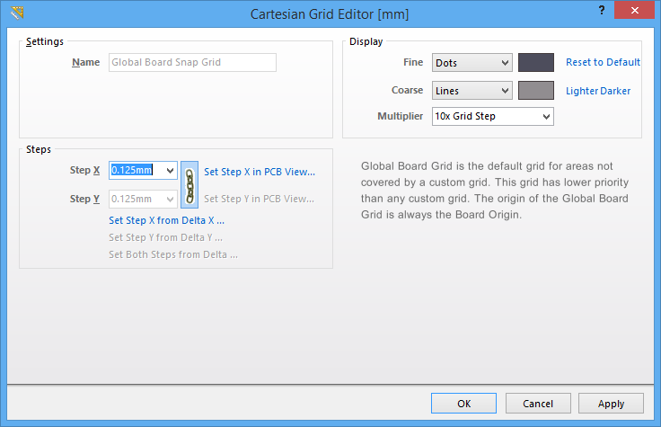
Set the Snap Grid to 0.125mm.
Component Positioning and Placement options
The next step is to set options that makes positioning components easier.
- Select Tools » Preferences (shortcut: T, P) to open the Preferences dialog. Open the PCB Editor - General page of the dialog, in the Editing Options section, make sure the Snap To Center option is enabled. This ensures that when you "grab" a component to position it, the cursor will hold the component by its reference point.
- Note the Smart Component Snap option, if this is enabled you can force the software to snap to a pad center instead of the reference point by clicking and holding closer to the required pad than the component's reference point. This is very handy if you require a specific pad, that is not the component's reference point, to be on a specific grid point, enable this option as well.
Enable Snap to Center to always hold the component by its reference point. Smart Component Snap is helpful when you need to align by pads.
- Switch to the PCB Editor - Interactive Routing page of the Preferences dialog.
- In the Interactive Routing Options section of the page, enable the Automatically Terminate Routing option. With this enabled, when a route reaches the target pad the cursor is automatically released from that net, ready to start routing another net.
- Confirm that the Automatically Remove Loops option is enabled. This option allows you to change existing routing by simply routing an alternate path - you route a new path until it meets the old path (creating a loop), then right-click to indicate it is complete - the software then automatically removes the old, redundant part of the routing.
- In the same page of the dialog, confirm that the Interactive Routing Width / Via Size Sources options are both set to Rule Preferred.
The PCB editor includes powerful interactive routing capabilities.
Setting Up the Design Rules
Main article: Design Rules
The PCB Editor is a rules-driven environment, meaning that as you perform actions that change the design, such as placing tracks, moving components, or autorouting the board, the software monitors each action and checks to see if the design still complies with the design rules. If it does not, then the error is immediately highlighted as a violation. Setting up the design rules before you start working on the board allows you to remain focused on the task of designing, confident in the knowledge that any design errors will immediately be flagged for your attention.
Design rules are configured in the PCB Rules and Constraints Editor dialog, as shown below. The rules fall into 10 categories, which can then be further divided into design rule types. The rules cover electrical, routing, manufacturing, placement, high speed and signal integrity design requirements.
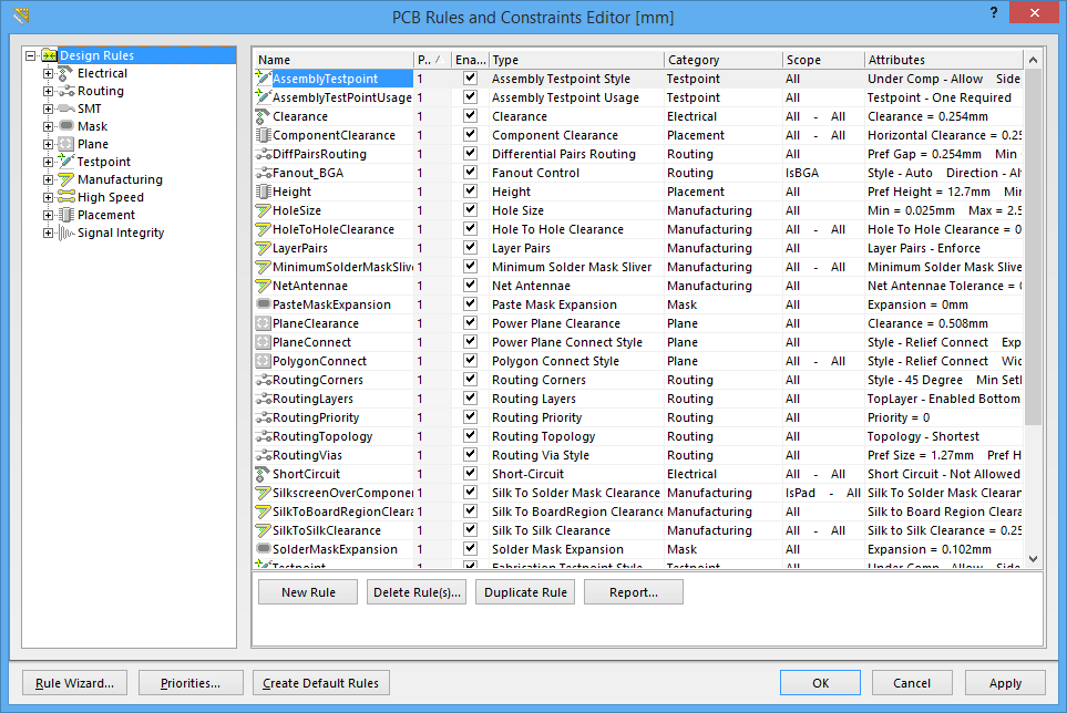
All PCB design requirements are configured as rules/constraints, in the PCB Rules and Constraints Editor.
Routing Width Design Rules
The tutorial design includes a number of signal nets, and two power nets. The default routing width rule (rule scope of All) will be configured for the signal nets, and another rule added to target the power nets.
Signal Nets Routing Width
To configure the default routing width rule:
- With the PCB as the active document, select Design » Rules from the menus.
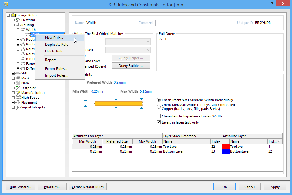
- The PCB Rules and Constraints Editor dialog will appear. Each rules category is displayed under the Design Rules folder (left hand side) of the dialog. Double-click on the Routing category to expand the category and see the related routing rules. Then double-click on Width to display the currently defined width rules.
- Click once on the existing Width rule to select it. When you click on the rule, the right hand side of the dialog displays the settings for that rule, including: the rule's Full Query (also referred to as its scope - what you want this rule to target) in the top section; and the rule's Constraints in the bottom section.
- Since this rule is to target the majority of nets in the design, the signal nets, setting the Full Query to
Allis appropriate. - The settings in this rule are the defaults for a new PCB, edit the Min Width, Preferred Width & Max Width values, setting them to 0.25mm. Note that you can configure the Width to be defined by impedance rather than a simple distance measurement. Note also that the settings are reflected in the individual layers shown at the bottom of the dialog, you can configure the requirements on a per-layer basis, essential when performing impedance controlled routing.
- The rule is now defined, click Apply to save it and keep the dialog open.
The default Routing Width design rule has been configured for the tutorial, a new rule is about to be added for power nets.
Power Nets Routing Width
We will now add and configure a new design rule to specify the width that the power nets must be routed. To set up this rule, complete the following steps:
- With the Width rule-type, or an existing Width rule selected in the Design Rules tree on the left of the dialog, right-click and select New Rule to add a new Width constraint rule.
- A new rule named Width_1 appears. Click on the new rule in the Design Rules tree to modify the scope and constraints.
- Click in the Name field on the right, and enter the name
Width_Powerin the field. - Next we will set the rule's scope using the Query Builder, to access this select the Advanced (Query) option. Note that you can always type the query in directly if you know the correct syntax. Alternatively, if your query is more complicated you could select the Advanced option, then click the Query Helper button to use the Query Helper dialog.
- Click the Query Builder button, then move through the steps to target objects in the 12V net OR the GND net. The animation below shows the process of using the Query Builder.
Using the Query Builder to create the Query, once that is done the required Width can be configured (shown in the next image).
- The Query Builder has been used to write a query that targets objects in the 12V net OR objects in the GND net. Alternatively, you could have created a Net Class containing those 2 nets (called
Powerfor example), then written a Query that targetted objectsInNetClass('Power'). - Now that the Query has been defined, the last step is to set the Constraints for the rule. Edit the Min Width / Preferred Width / Max Width values
0.25/0.5/0.5to allow power net routing widths in the range 0.25mm to 0.5mm, as shown in the image below.
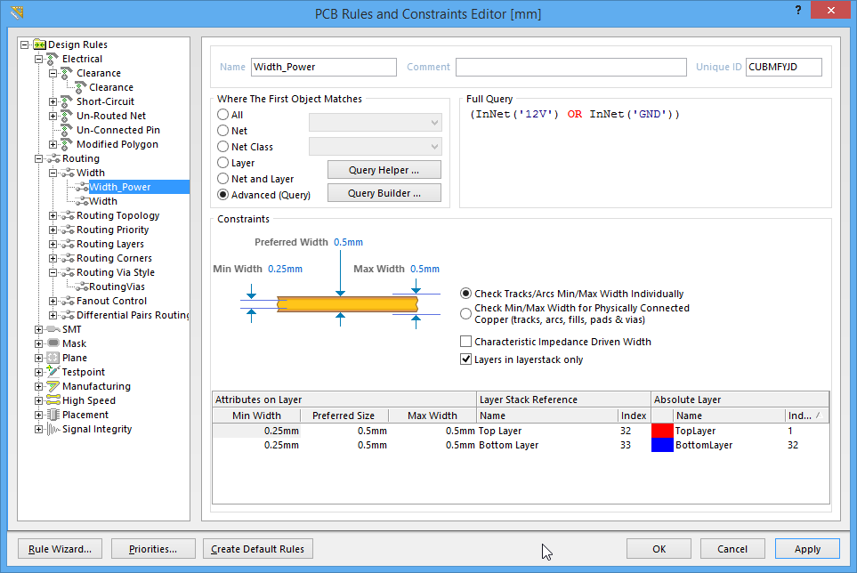
This Width rule targets the power nets.
- Click Apply to save the rule and keep the dialog open.
Defining the Electrical Clearance Constraint
The next step is to define how close electrical objects that belong to different nets, can be to each other. To do this:
- Expand the Electrical category in the tree of Design Rules, then expand the Clearance rule-type.
- Click to select the existing Clearance constraint. Note that this rule has two Full Query fields, that is because it is a Binary rule. The rules engine checks each object targeted by the first Full Query, and checks them against the objects targeted by the second Full Query, to confirm that they satisfy the specified Constraints setting. For this design, it is suitable to define a single clearance between
Allobjects. - In the Constraints region of the dialog, set the Minimum Clearance to
0.25mm, as shown in the image below.
![]()
Configure the electrical clearance to be 0.25mm.
- Click Apply to save the rule and keep the dialog open.
Defining the Routing Via Style
The last rule to define is the Routing Via Style. To do this:
- Expand the Design Rule tree and select the default RoutingVias design rule.
- Since it is highly likely that the power nets can be routed on a single side of the board, it is not necessary to define a via for signal nets and another via for power nets. Edit the rule settings to the values defined earlier in the turorial, that is a Via Diameter =
1mmand a Via Hole Size =0.6mm. Set all fields (Min, Max, Preferred) to the same size.Note that you can press Tab on the keyboard to move from one dialog field to the next.
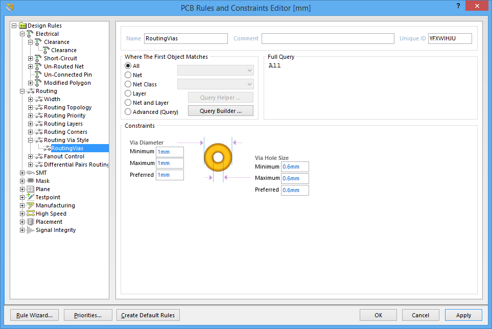
A single routing via is suitable for all nets in this design.
- Click OK to close the PCB Rules and Constraints Editor.
- Save the PCB file.
Positioning the Components on the PCB
There is a saying that PCB design is 90% placement and 10% routing. While you could argue about the percentage of each, it is generally accepted that good component placement is the most important aspect to good board design. Keep in mind that you may need to tune the placement as you route too.
We can now start to place the components in suitable locations on the board.
- Press the V, D shortcut keys to zoom in on the board and components.
- If you need to zoom in, you can then press PageUp; or Ctrl+Roll; or hold Ctrl then Right-click-and-hold to display the zoom cursor, and move the mouse up. All zooming is relative to the current cursor location, position the cursor before zooming.
- The components will be positioned on the current Snap grid, which is 0.125mm. As the designer you decide what a suitable placement grid is, for a simple design such as this there are no design requirements that dictate what an appropriate placement grid might be. To simplify the process of positioning the components, you can work with a coarse placement grid, for example 1mm. To change the grid, press Ctrl+G to open the Cartesian Grid Editor, type the value
1mminto the Step X field, and click OK to close the dialog.
- The components in the tutorial will be placed as shown in the image below. To place connector
Y1, position the cursor over the middle of the outline of the connector, and Click-and-Hold the left mouse button. The cursor will change to a cross hair and jump to the reference point for the part. While continuing to hold down the mouse button, move the mouse to drag the component. -
Position the footprint towards the left-hand side of the board (ensuring that the whole of the component stays within the board boundary), as shown in the figure below.
Components positioned on the board.
- When the connector component is in position, release the mouse button to drop it into place. Note how the connection lines drag with the component.
- Reposition the remaining components, using the figure above as a guide. Use the Spacebar to rotate (increments of 90º anti-clockwise) components as you drag them, so that the connection lines are as shown in the figure.
- Component text can be repositioned in a similar fashion - click-and-drag the text and press the Spacebar to rotate it.
- The PCB editor also includes powerful interactive placement tools. Let's use these to ensure that the four resistors are correctly aligned and spaced.
- Holding the Shift key, click on each of the four resistors to select them, or click and drag the selection box around all 4 of them. A shaded selection box will display around each of the selected components in the color set for the system color called Selections. You can change this selection color in the View Configurations dialog (Design » Board Layers & Colors, or the L shortcut).
-
Right-click on any of the selected components and choose Align » Align (shortcut: A, A). In the Align Objects dialog, click on Space Equally in the Horizontal section and click on Top in the Vertical section. Click OK to apply these changes, the four resistors are now aligned and equally spaced.
Align and space the resistors.
- Click elsewhere in the design window to de-select all the resistors. If required you can also align the capacitors and transistors, although this might not be required since you have a coarse Snap grid at the moment.
Changing a Footprint
Now that we have positioned the footprints, we can see the capacitor footprint is too big for our requirements! Let's change the capacitor footprint to a smaller one.
- Double-click on one of the capacitors to open the Component dialog.
-
In the Footprint region of the dialog, you will see that the current footprint Name is RAD-0.3. To choose another footprint, click the ... button, as shown in the figure below, to open the Browse Libraries dialog and choose a different footprint.
Click to select a different footprint.
- In the Browse Libraries dialog, click the dropdown arrow in the Libraries field to display the list of currently installed libraries, ensure that the Miscellaneous Devices.IntLib is selected.
- We want a smaller radial type footprint, so type
radin the Mask field of the dialog to display only the radial style footprints.
Search the current library for a suitable footprint.
- RAD-0.1 will be suitable, select it and click OK to close the Browse Libraries dialog, then click OK again to close the Component dialog. The capacitor should show the new smaller footprint.
- Repeat the process for the other capacitor.
- Reposition the designators as required.
- Save the PCB file.
Your board should now look something like the figure below.
Components placed on the board with new footprints.
With everything positioned, it's time to do some routing!
Interactively Routing the Board
Main articles: Getting ready to route, Interactively Routing a Net, Modifying Existing Routing
Routing is the process of laying tracks and vias on the board to connect the component pins. The PCB editor makes this job easy by providing sophisticated interactive routing tools as well as the Situs topological autorouter, which optimally routes the whole or part of a board at the click of a button.
While autorouting provides an easy and powerful way to route a board, there will be situations where you will need exact control over the placement of tracks. In these situations you can manually route part or all of your board. In this section of the tutorial, we will manually route the entire board single-sided, with all tracks on the bottom layer. The Interactive Routing tools help maximize routing efficiency and flexibility in an intuitive way, including cursor guidance for track placement, single-click routing of the connection, pushing or walking around obstacles, automatically following existing connections, all in accordance with applicable design rules.
As we place tracks on the bottom layer of the board, we will use the ratsnest (connection lines) to guide us. Tracks on a PCB are made from a series of straight segments. Each time there is a change of direction, a new track segment begins. Also, by default the PCB editor constrains tracks to a vertical, horizontal or 45° orientation, allowing you to easily produce professional results. This behavior can be customized to suit your needs, but for this tutorial we will use the default.
- Before starting routing, we need to confirm that the grid is appropriate for routing. To change the grid, press Ctrl+G to open the Cartesian Grid Editor, type the value
0.125mminto the Step X field, and click OK to close the dialog. - Check which layers are currently visible by looking at the Layer Tabs at the bottom of the workspace. If the Bottom Layer is not visible, press the L shortcut to open the View Configurations dialog, and enable the Bottom Layer.
- Click on the Bottom layer tab at the bottom of the workspace to make it the current, or active layer, ready to route on.
- It is often easier to route in single layer mode, press Shift+S to toggle to single layer mode (repeat to cycle through the enabled single layer modes - the modes are configured in the PCB Editor - Board Insight Display page of the Preferences dialog).
- Select Place » Interactive Routing from the menus (shortcut: P, T), or click the Interactive Routing button , or right-click and choose Interactive Routing from the context menu. The cursor will change to a crosshair, indicating you are in interactive routing mode.
- Position the cursor over the lower pad on connector Y1. As you move the cursor close to the pad it will automatically snap to the center of the pad - this is the Snap To Object Hotspot feature pulling the cursor to the center of the nearest electrical object (configure the Range of attraction in the Board Options dialog). Sometimes the Snap To Object Hotspot feature pulls the cursor when you don't want it to, in this situation press the Ctrl key to temporarily inhibit this feature.
- Left-Click or press Enter to anchor the first point of the track.
- Move the cursor towards the bottom pad of the resistor R1, and click to place a vertical segment. Note how track segments are displayed in different ways (as shown in the image below). During routing, the segments are shown as:
- Solid - the segment has been placed.
- Hatched - hatched segments are proposed but uncommitted, they will be placed when you left-click.
- Hollow - this is referred to as the look-ahead segment, it allows you to work out where the last proposed segment should end. If you are routing in free space the look-ahead segment is not placed when you click. If you have the Automatically Terminate Routing option on (this was enabled earlier), then the look-ahead segment is placed together with the hatched segment(s), if the click event occurs on the target pad.
Note how the segments are displayed differently.
- Manually route by Left-Clicking to commit track segments, finishing on the lower pad of R1. Note how each mouse click places the hatched segment(s). For the connection that you are currently routing:
- Press Backspace to rip up the last-placed segment.
- Move your cursor back along the path, as soon as you pass over an existing uncommitted segment, the uncommitted routing unwinds back to this location.
- Rather than routing all the way to the target pad, you can also press Ctrl+Left Click to use the Auto-Complete function and immediately route the entire connection. Auto-complete behaves in the following way:
- It takes the shortest path, which may not the best path as you need to always consider paths for other connections yet to be routed. If you are in Push mode (shown on the Status bar when routing), Auto-complete can push existing routes to reach the target.
- On longer connections, the Auto-Complete path may not always be available as the routing path is mapped section by section and complete mapping between source and target pads may not be possible.
- You can also Auto-complete directly on a pad or connection line.
- Continue to route all the connections on the board. To unroute, press U to pop up the Unroute sub-menu, then choose the required option. Track dragging and rerouting will be discussed shortly.

Cursor following streamlines the manual routing process. committed tracks display in solid color, uncommitted tracks are shown hatched\hollow.
- Use the techniques detailed above to route between the other components on the board. The simple animation below shows the board being interactively routed.
- There is no single solution to routing a board, so it is inevitable that you will want to change the routing. The PCB editor includes features and tools to help with this, they are discussed in the following sections.
- Save the design when you are finished.
Animation showing the board being interactively routed, with all tracks placed on the bottom layer. Press the Spacebar to toggle the corner direction.
Routing Tips
Keep in mind the following points as you are routing:
- Keep an eye on the Status bar, it displays a lot of important details, which are listed below.
- While routing, press ~ (tilda) or Shift+F1 for a list of interactive shortcuts - most settings can be changed on the fly by pressing the appropriate shortcut, or selecting from the menu that appears.
- Press * on the numeric keypad while routing to cycle through the available signal layers. A via will automatically be added, in accordance with the applicable Routing Via Style design rule. Alternatively, use Ctrl+Shift+Roll shortcuts to move back and forth through the available signal layers.
- Shift+R to cycle through the enabled conflict resolution modes, including Push, Walkaround, Hug and Push, and Ignore. Enable the required modes in the PCB Editor - Interactive Routing page of the Preferences dialog.
- Shift+S to cycle single layer mode on and off, ideal when there are many objects on multiple layers.
- Spacebar to toggle the corner direction (for all but any angle mode).
- Shift+Spacebar to cycle through the various track corner modes. The styles are: any angle, 45°, 45° with arc, 90° and 90° with arc. There is an option to limit this to 45° and 90° in the PCB Editor - Interactive Routing page of the Preferences dialog.
- Ctrl+Left-Click at any time to Auto-complete the connection. Auto-complete will not succeed if there are unresolvable conflicts with obstacles.
- Ctrl to temporarily suspect the Hotspot Snap (formerly called the Electrical Grid), press Shift + E to cycle through the 3 available modes (off / on for current layer / on for all layers).
- END at any time to redraw the screen.
- V, F at any time to redraw the screen to fit all objects.
- PageUp and PageDown keys at any time to zoom in or out, centered on the cursor position. Alternatively, use the standard Windows mouse wheel zoom and pan shortcuts.
- Backspace to remove the last-committed track segments.
- Right-click or press ESC when you have finished placing a track and want to start a new one.
- To unroute, press U to open the Unroute menu, then select the required command (Net, Connection, Component, Room).
- When you start a route you can click on the pad or click on the connection line, and you can stop routing anywhere. As soon as you right-click to finish that route, the routing is analyzed and the connection lines are updated and removed as required.
Interactive Routing Modes
Main article: Interactively Routing a Net
The PCB editor's Interactive Routing engine supports a number of different modes, with each mode helping the designer deal with particular situations. Press the Shift + R shortcut to cycle through these modes as you interactively route, note that the current mode is displayed on the Status bar.
The available modes include:
- Ignore - This mode lets you place tracks anywhere, including over existing objects, displaying but allowing potential violations.
- Stop at first obstacle - In this mode the routing is essentially manual, as soon as an obstacle is encountered the track segment will be clipped to avoid a violation.
- Walkaround - This mode will attempt to find a routing path around existing obstacles without attempting to move them.
- Push - This mode will attempt to move objects (tracks and vias), which are capable of being repositioned without violation, to accommodate the new routing.
- Hug & Push - This mode is a combination of Walkaround and Push. It will hug as it performs a Walkaround of obstacles, however, will also attempt to Push against fixed obstacles when there is insufficient clearance to continue using Walkaround.
- Autoroute on Current Layer - this mode brings basic autorouting functionality to interactive routing, it can automatically select between walkaround and push, based on heuristics that consider push distance, versus walk distance and route length. Like an autorouter, this mode can deliver better results on a complex, busy board, than on a simple, unrouted board.
- Autoroute on Multiple Layers - this mode also brings basic autorouting functionality to interactive routing, it can also automatically select between walkaround and push, based on heuristics that consider push distance, versus walk distance and route length. This mode can also place a via and consider using other routing layers. Like an autorouter, this mode can deliver better results on a complex, busy board, than on a simple, unrouted board.
Modifying and Rerouting
Main article: Modifying Existing Routing
Given that board design is a highly fluid process, you will find that the routes that seemed great today may no longer be suitable tomorrow, so it is essential to understand how to re-route and modify existing routes.
Because we originally defined our board as being double-sided in the PCB Board Wizard, you could manually route your board double-sided using both the top and bottom layers. To do this, un-route the board by selecting Tools » Un-Route » All from the menus. Start interactive routing as before, to switch routing layers press the * key on the numeric keypad to toggle between the layers while placing tracks, or use the Ctrl+Shift+Roll keys/mouse to move back and forth through the available signal layers as you route. The PCB editor will automatically insert a via (in accordance with the Routing Via design rule) as necessary when you change layers.
To modify an existing route, there are two approaches: reroute, or re-arrange.
Reroute an existing Route
There is no need to un-route a connection to redefine its path, simply select Place » Interactive Routing and start re-routing, the Loop Removal feature will automatically remove any redundant track segments (Loop Removal was enabled earlier in the tutorial). The PCB editor includes a net analyzer that automatically analyses the route path as you work and removes redundant segments and vias. You can start and end the new route path at any point, swapping layers as required.
Animation showing the Loop Removal feature being used to modify existing routing.
Re-arrange Existing Routes
You can also interactively slide or drag track segments across the board to make room for new routes. The PCB editor will automatically maintain the 45/90 degree angles with connected segments, shortening and lengthening them as required.
To drag a segment:
- Click once to select the segment, position the mouse over the segment to display the quad-arrow cursor, then Click and hold to start dragging that segment. Note that the cursor changes if you position it over the center track vertex - this is a different mode, used to break a single segment into 3 segments.
- Alternatively, instead of selecting the segment first, Ctrl + Click and hold on a segment to start dragging that segment.
Animation showing track dragging in push mode, the via is automatically jumped.
Track Dragging Tips
- During dragging the routing conflict resolution modes apply (Ignore, Push, Hug and Push), press Shift + R to cycle through the modes as you drag a track segment.
- Existing pads and vias will be jumped, or vias will be pushed if necessary and possible.
- To convert a 90 degree corner to a 45 degree route, start dragging on the corner vertex.
- While dragging you can move the cursor and hotspot snap it to an existing, non-moving object such as a pad, use this to help align the new segment location with an existing object and avoid very small segments being added.
- Position the cursor over the track segment center vertex to add in new segments.
- Change the default select-then-drag mode using the Unselected via/track and Selected via/track options in the PCB Editor - Interactive Routing page of the Preferences dialog.
Automatically Routing the Board
Main article: Situs Autorouting Essentials
To see how easy it is to autoroute, complete the following steps:
- Un-route the board by selecting Tools » Un-Route » All from the menus (shortcut: U, A).
- Select Auto Route » All. The Situs Routing Strategies dialog displays, the top region of the dialog displays the Routing Setup Report, warnings and errors are shown in red, always check for warnings/errors. The lower half of the dialog shows the available Routing Strategies, the selected one will be highlighted. For this board it should default to the Default 2 Layer Board strategy.
- Click on Route All in the Situs Routing Strategies dialog. The Messages panel displays the process of the autorouting. The Situs autorouter is a topological autorouter, producing results comparable with that of an experienced board designer. Because it routes your board directly in the PCB editing window, there is no need to wrestle with exporting and importing route files.
- To route the board single-sided, click the Edit Layer Directions button in the Situs Routing Strategies dialog, and modify the Current Setting field. Alternatively you can modify the Routing Layers design rule.
- An interesting point to make, the Situs router prefers a challenging board, often giving better results on a dense, complex design than on a simple board. To improve the quality of the finished result, select Auto Route » All again, except this time select the Cleanup routing strategy. This strategy will attempt to straighten the routes, reducing the number of corners. You can run the Cleanup strategy multiple times if required. If nothing changes you might like to interactively re-route a connection in a convoluted pattern, then try the Cleanup strategy.
- Select File » Save (shortcut: F, S) to save your board.
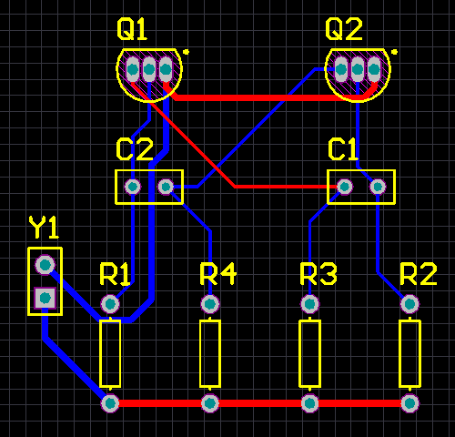
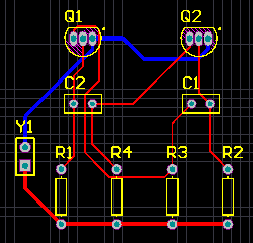
Fully autorouted board, left image shows layers set to Top-horizontal / Bottom-vertical, right image shows Top-horizontal / Bottom-horizontal.
The autorouter will route on both the top and bottom layers, red tracks on the top layer, blue on the bottom layer. The layers that are used by the autorouter are specified in the Routing Layers design rule, which defaults to top and bottom layers. Also notice the two power net tracks running from the connector are wider, as specified by the second Width design rule you set up.
Verifying Your Board Design
Main article: Design Rule Checking
The PCB editor is a rules-driven board design environment, in which you can define many types of design rules to ensure the integrity of your board. Typically, you set up the design rules at the start of the design process and then verify that the design complies with the rules as you work through the design, and again at the end of the design process.
Earlier in the tutorial we examined the routing design rules, adding a new width constraint rule targeting the power nets, as well as an electrical clearance constraint and a routing via style rule.
Configuring the Display of Rule Violations
- Select Design » Board Layers & Colors (shortcut: L) and ensure that Show checkbox next to the DRC Error Markers option in the System Colors section is enabled (ticked) so that DRC error markers will be displayed.
- Confirm that the Online DRC (Design Rule Checking) system is enabled, the checkbox is in the PCB Editor - General page of the Preferences dialog. Keep the Preferences dialog open, and switch to the PCB Editor - DRC Violations Display page of the dialog.
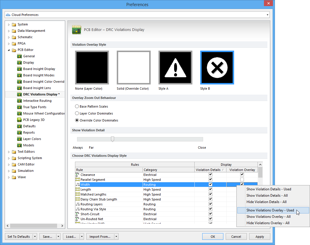
Violations can be displayed as a colored overlay and also as a detailed message, with different symbols being used to show different detail of the error type.
- The PCB Editor - DRC Violations Display page of the Preferences dialog is used to configure how violations are displayed in the workspace. There are 2 different methods available for displaying violations, each with their own strengths:
- Violation Overlay - Violations are identifed by the primitive that is in error being highlighted in the color chosen for the DRC Error Markers (checked in step 1 just above). The default behavior is to show the primitives in a solid color when zoomed out, changing to the selected Violation Overlay Style as you zoom it. The default is Style B, a circle with a cross in it.
- Violation Details - As you zoom further in Violation Detail is added (if enabled), detailing the nature of the error. In the images below the Violation Detail is < 0.254, meaning the distance between the soldermask and the silkscreen is less that the applicable rule setting of 0.254. The Heads Up display can display information about violations, it shown as a violation of the Silk to Soldermask clearance constraint. Use the Show Violation Detail slider to define at what zoom level the Violation Details are displayed. The images below show how the display changes at different zoom levels, click to enlarge.
- For the tutorial, right-click in the Display area of the PCB Editor - DRC Violations Display page of the Preferences dialog and select Show Violation Details - Used, then right-click again and select Show Violation Overlay - Used, as shown in the image above.
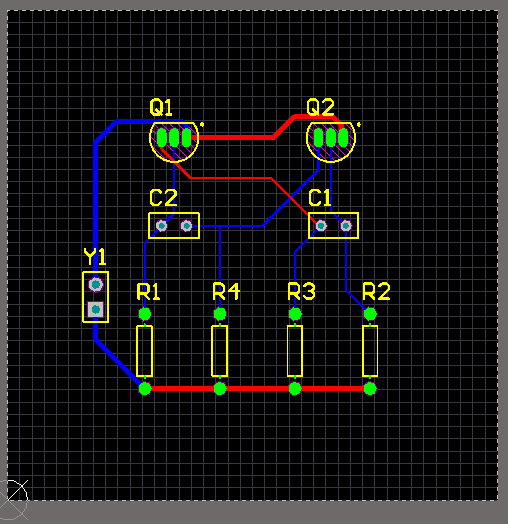


Violations are shown in solid green (left image), as you zoom in an Overlay is added (center image), as you zoom in further Violation Details are added.
- You are now ready to check the design for errors.
Checking for Rule Violations
To verify that the routed circuit board conforms to the design rules, we will now run a Design Rule Check (DRC):
- Select Tools » Design Rule Check (shortcut: T, D) to open the Design Rule Checker dialog. Both the online and batch DRC options are configured in this dialog. By default, the dialog opens showing the Report Options selected in the tree on the left of the dialog (as shown in the image below). The right of the dialog displays a list of general reporting options, press F1 when the cursor is over the dialog for more information (try a second time if it fails to load the first time). These options will be left at their defaults.
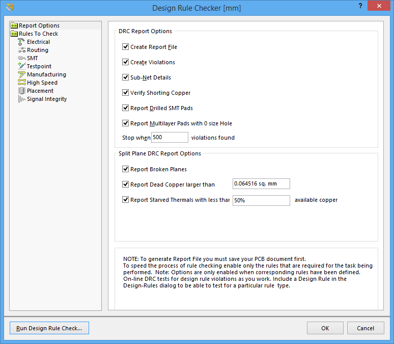
Rule checking, both online and batch, is configured in the Design Rule Checker dialog.
- Click on the Rules to Check in the list on the left of the dialog, all of the rule types will be listed. You can narrow the list by clicking on a specific category, for example Electrical, to see all the rules belonging to that category. For most rule types there are checkboxes for Online (check as you work) and Batch (check when the Run Design Rule Check button is clicked)
- If it is not currently selected, switch back to the Rules to Check page in the tree on the left of the dialog. Then in the list of rules on the right-side of the dialog, right-click to display the context menu. This menu allows you to quickly toggle the Online and Batch settings, select the Batch DRC - Used On entry, as shown in the image below.

Checking is configured for each rule type, use the right-click menu to toggle multiple options.
- Click the Run Design Rule Check button down the bottom left of the dialog. The DRC will run, the Messages panel will appear, and the Design Rule Verification Report will open in a separate document tab, an example is shown below.
The report details all detected violations, click on a violation to jump back to the PCB and examine the error.
- Scroll down through the report, noting that 2 types of rule violations have been detected, Silk To Solder Mask and Minimum Solder Mask Sliver. Below the summary of violating rules will be specific details about each violation.
- The links in the report are live, click on an error to jump back to the board and examine that error on the board. Note that the zoom level for this click action is configured in the System - Navigation page of the Preferences dialog, experiment to find a setting that suits you.
Identifying the Error Conditions
- When you are new to the software, a long list of violations can initially seem overwhelming. A good approach to managing this is to disable and enable rules in the Design Rule Check dialog, at different stages of the design process (it is not advisable to disable the design rules themselves, just the checking of them). For example, you would always disable the Un-Routed Net check until the board is fully routed. You might also disable all Manufacturing rule checks until you have completed the placement and routing, and finished checking of the placement and routing rules.
- When a batch DRC is run on the tutorial board, there are 8 silk to solder mask violations, and 4 solder mask sliver violations - which means the measured values are less than the minimum amounts specifed in those design rules. You now know how to locate those violations (click the link in the report file, or double click in the Messages panel), the next step is to work out what the actual value is so you know how much it has failed by. The image below shows the Violation Details for a silk to solder mask error, indicated by the white arrows and the
0.254mmtext. The cursor is also being hovered over the violating pad so that the Heads Up Display (HUD) can be used to show details of what rule is in error, as well as the measured value and the rule setting. Note that the HUD details the actual clearance (0.14mm), which you need to know to be able to make a decision about how to resolve it. The HUD is toggled on and off using the Shift+H shortcut, and HUD cursor tracking is toggled on and off using the Shift+G shortcut. The HUD display content is configured in the PCB Editor - Board Insight Modes page of the Preferences dialog.
The Heads Up display details that it is a Silk to Solder Mask Clearance violation, between a track and a pad. It does not detail the actual clearance though.
- Another approach to locating and understanding design rule violations is to use the PCB Rules and Violations panel (click the PCB button down the bottom right of the workspace to enable it). The image below shows the panel, locate the Silk to Solder Mask Clearance Constraint in the list.
- Click once on a Violation to jump to that violation, double-click on a violation to open the Violation Details dialog.
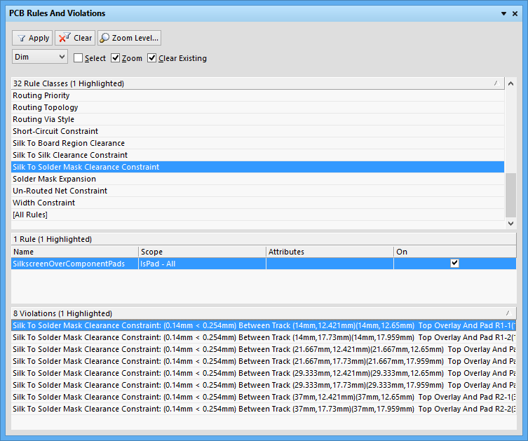
The panel details the violation type, the measured value, the rule setting and the objects that are in violation.
- Note that the Violation selected in the panel (image above) states that the clearance is
0.14mm < 0.254mm. - To resolve this violation we can either:
- Modify the silkscreen in the footprint in the Library editor to increase the clearance, or
- Decrease the mask expansion in the Solder Mask Expansion design rule to increase the clearance, or create a second rule that decreases it for just the resistor footprint as it is the only footprint showing this violation.
- Open the PCB Rules and Constraint Editor (Design » Rules), then locate and select the Silk to Solder Mask Clearance constraint, as shown in the image below.
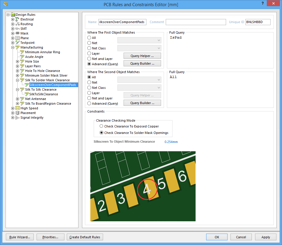
The Silk to Solder Mask constraint defines how far silk objects must be from either: the solder mask opening, or the underlying copper exposed by that opening.
- The current value of 0.254mm (10mil) is conservative, especially since the rule is configured to check the silk against the solder mask opening rather than the underlying copper. Half of the current value would still be an appropriate value for low-cost fabrication. Set the Silkscreen to Object Minimum Clearance to
0.125mmin the dialog, and click OK. - Time to run a DRC again, open the Design Rule Checker (Tools » Design Rule Check), this time disable the Create Report File option, then click the Run Design Rule Check button.
- The violations on the resistor pads should now be gone, the Messages panel should now only show four Minimum Solder Mask Sliver Constraint violations. If it is not visible, open the PCB Rules and Violations panel again, click on the Minimum Solder Mask Sliver Constraint in the upper list, then click on one of 4 violations detailed in the lower section of the panel.
- This violation is saying that the width of the strip of solder mask running between the transistor pads is
0.067mm, considerably less than the0.254mmcurrently specified in the rule. - To resolve this violation we can either:
- Increase the solder mask opening to completely remove the mask between the transistor pads, or
- Decrease the minimum acceptable sliver width, or
- Decrease the mask opening to widen the sliver to an acceptable width.
- This is a design decision which would be made in light of your knowledge of the component, and the fabrication and assembly technology being used. Opening the mask to completely remove the mask between the transistor pads means that there is more chance of creating solder bridges between those pads, whereas decreasing the mask opening will still leave a sliver which may or may not be acceptable, and will also introduce the possibility of mask-to-pad registration problems. For this tutorial we will do a combination of the second and third options, decreasing the minimum sliver width to a value suitable for the settings being used on this board, and also decreasing the mask expansion, but only for the transistor pads.
- The first step is to reduce the allowable sliver width. To do this, open the PCB Rules and Constraints Editor dialog (Design » Rules), then in the Manufacturing section locate and select the existing Minimum Solder Mask Sliver rule, called MinimumSolderMaskSliver.
- A value of 0.125mm (5mil) should be acceptable for a design such as this, edit the Minimum Solder Mask Sliver value to
0.125mmin the Constraints region of the rule. - Now click on Mask in the tree on the left of the dialog to show the current Solder Mask Expansion rules, there should be one called SolderMaskExpansion. Click on it to select the rule and display its settings, it will specify an expansion value of 0.102mm (4mil). We only want to change this for the transistors so we will not edit this value, instead we will create a new rule.
- To add a new Solder Mask Expansion rule, right-click on the current rule and select New Rule. A new rule called SolderMaskExpansion_1 will be created, click on it to display its settings.
- Edit the rule settings to be:
- Name - SolderMaskExpansion_TO-92A
- Full Query - HasFootprint('TO-92A')
- Expansion - 0.07mm
- Click OK to close the PCB Rules and Constraints Editor dialog, then select Tools » Design Rule Check and run the batch design rule check again. If online checking is enabled for this rule type, you will not need to run the batch rule check.
- When rules checking is complete there should be no violations present in the design, reflected by an empty Messages panel. If a report was needed that showed the design has no errors, you could re-enable the Create Report File option in the Design Rule Check dialog.
Well done! You have completed the PCB layout and are ready to produce output documentation. Before doing that, we'll explore the PCB editor's 3D capabilities.
Viewing Your Board in 3D
Related tutorial: Creating Library Components Tutorial
Related articles: Working with the Board Insight System, ECAD - MCAD Integration
Now that your board design is complete, let's examine it as a 3 dimensional object. To switch to 3D, select View » 3D Layout Mode (shortcut: 3), or select a 3D view configuration from the list on the PCB Standard toolbar. The board will display as a 3 dimensional object.
You can fluidly zoom the view, rotate it and even travel inside the board using the following controls:
- Zooming - Ctrl + Right-drag mouse, or Ctrl + Roll mouse-wheel, or the PageUp / PageDown keys.
- Panning - Right-drag mouse, or the standard Windows mouse-wheel controls.
- Rotation - Shift + Right-drag mouse. Note how when you press Shift a directional sphere appears at the current cursor position, as shown in the figure below. Rotational movement of the model is made about the center of the sphere (position the cursor before pressing Shift to position the sphere) using the following controls. Move the mouse around to highlight and select each one:
- Right-drag sphere when the Center Dot is highlighted - rotate in any direction.
- Right-drag sphere when the Horizontal Arrow is highlighted - rotate the view about the Y-axis.
- Right-drag sphere when the Vertical Arrow is highlighted - rotate the view about the X-axis.
- Right-drag sphere when the Circle Segment is highlighted - rotate the view about the Z-plane.
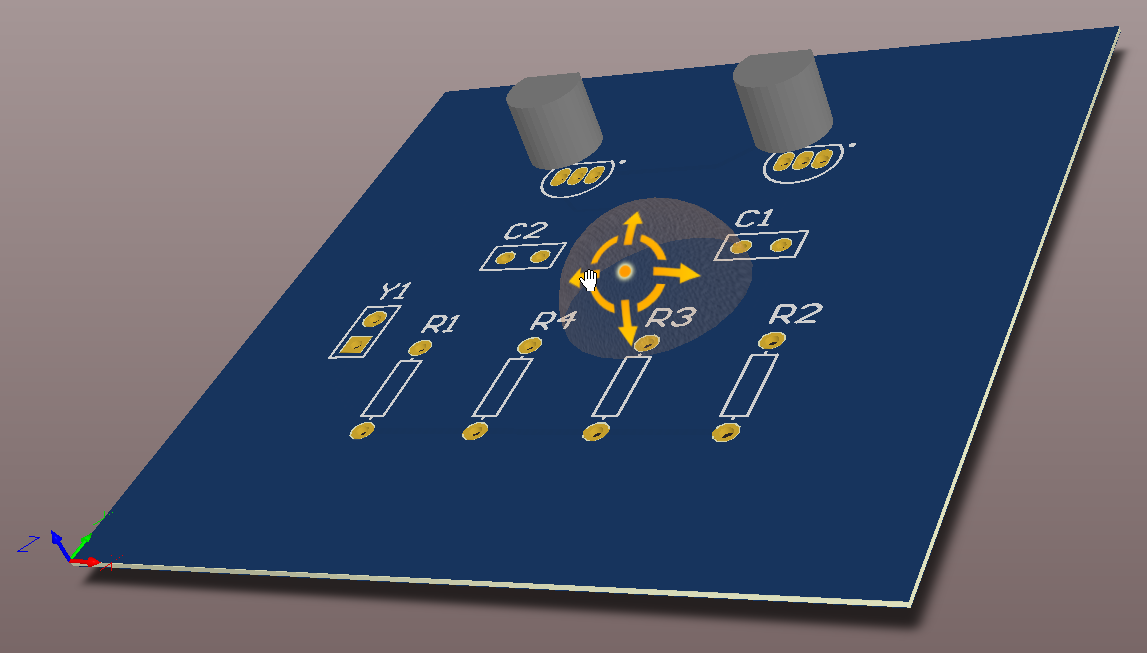
Hold Shift to display the 3D view directiional sphere, then click and drag the right-mouse button to rotate.
Tips for Working in 3D
- You can configure 3D workspace display options using the View Configurations dialog (shortcut: L) when the board is in 3D Layout Mode. There are options to choose various surface and workspace colors as well as vertical scaling, which is handy for examining the PCB internally. Some surfaces have an opacity setting - the greater the opacity, the less 'light' passes through the surface, which makes objects behind less visible. You can also choose to show 3D bodies or render 3D objects in their (2D) layer color.
- To display the components in 3D, each component needs to have a suitable 3D model. You can import 3D STEP-format models into component footprints, or you can create your own component shape by placing 3D Body Objects in the footprint in the library editor. Check out 3D Content Central for STEP format component models. For more information on creating 3D bodies for components, refer to the Including Three-Dimensional Component Detail section of the Creating Library Components Tutorial.
- To export the 3D PCB in STEP format, select File » Export.
- You can create a clipboard snapshot of the current view in 3D mode, click once on the workspace and press Ctrl + C. Select the required resolution in the 3D Snapshot Resolution dialog, the image is loaded into the Windows clipboard in bitmap format, ready for use in other applications. If the 3D Snapshot Resolution dialog does not appear, select a 3D body first, then try again.
- You can import an enclosure designed in an MCAD application into the PCB editor and check the board for fit. For more information on integration with MCAD applications refer to the Integrating MCAD Objects and PCB Designs tutorial. The tutorial uses the same multivibrator design.
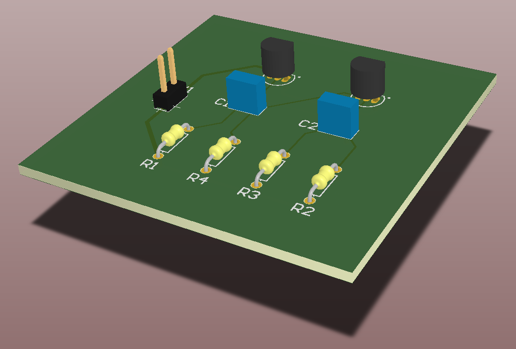
The Multivibrator PCB complete with components - 3D Bodies have been used for the transistors and caps, STEP models for the resistors and header.
The Multivibrator PCB fully assembled into a two part housing assembly, displayed in the PCB editor's 3D Layout mode.
Output Documentation
Related articles: Design to Manufacturing, Fabrication Outputs
Now that you've completed the design and layout of the PCB, you will want to produce output documentation to get the board reviewed, manufactured and assembled. Output settings can be configured from within the PCB editor, these settings will be stored in the project file. Output settings can also be configured in an Output Job File, a dedicated output settings document.
The advantages of using an Output Job (OutJob) include:
- Full control over the naming of output files/folders, and the folder structure of the outputs.
- Multiple outputs of the same type can be configured, ideal if multiple fabricators are being considered.
- Multiple OutJobs can be included in the project, allowing outputs to be organized to suit your design and your company.
- PDF outputs can be collated, or output into separate files.
- Outputs can be configured and generated for each Variant, if Variants are defined.
- Output settings can be copied from one project to another by copying the OutJob.
- Outputs can be manually managed, or release managed - where the software manages their generation and storage in an Altium Vault.
- Outputs can be generated without needing to open the schematics or PCB file, ideal if different staff handle that stage of the process.

OutJobs allow easy access to all outputs, with full control over their settings.
To add an OutJob to the project:
- In the Projects panel, right click on the project name and select Add New to Project » Output Job File. A new OutJob will be opened and added to the project.
- Save the OutJob and name it Multivibrator. It will automatically be saved in the same folder as the project file.
- To add a new Gerber output, click the link in the Fabrication Outputs section of the OutJob, and select Gerber » [PCB Document], as shown in the image below. You can select the generic [PCB Document] option if there is only one board in the project, it will automatically be chosen for generation. This makes the OutJob more easily copied between projects, as this setting will not have to be updated. If there are multiple PCBs in the project you will need to select the specific board.
- The Gerber output has been added, you will configure it shortly.
Adding a Gerber output into the OutJob.
Available Output Types
Because a variety of technologies and methods exist in PCB manufacture, the software has the capability to produce numerous output types for different purposes:
- Assembly Drawings - component positions and orientations for each side of the board.
- Pick and Place Files - used by robotic component placement machinery to place components onto the board. Note that the Report Output can also be used to generate Pick and Place files, and is highly configurable.
- Composite Drawings - the finished board assembly, including components and tracks.
- PCB 3D Prints - views of the board from a three-dimensional view perspective.
- Schematic Prints - schematic drawings used in the design.
- Composite Drill Drawings - drill positions and sizes (using symbols) for the board in one drawing.
- Drill Drawing/Guides - drill positions and sizes (using symbols) for the board in separate drawings.
- Final Artwork Prints - combines various fabrication outputs together as a single printable output.
- Gerber Files - creates manufacturing information in Gerber format.
- Gerber X2 Files - a new standard that encapsulates a high-level of design information, with backward compatibility to the original Gerber format.
- IPC-2581 File - a new standard that encapsulates a high-level of design information within a single file.
- NC Drill Files - creates manufacturing information for use by numerically controlled drilling machines.
- ODB++ - creates manufacturing information in ODB++ database format.
- Power-Plane Prints - creates internal and split plane drawings.
- Solder/Paste Mask Prints - creates solder mask and paste mask drawings.
- Test Point Report - creates test point output for the design in a variety of formats.
- Netlists describe the logical connectivity between components in the design and is useful for transporting to other electronics design applications.
- Bill of Materials - creates a list of parts and quantities (BOM), in various formats, required to manufacture the board.
- Component Cross Reference Report - creates a list of components, based on the schematic drawing in the design.
- Report Project Hierarchy - creates a list of source documents used in the project.
- Report Single Pin Nets- creates a report listing any nets that only have one connection.
- Simple BOM - creates text and CSV (comma separated variables) files of the BOM.
Generating Gerber Files
Each Gerber file corresponds to one layer of the physical board - the component overlay, top signal layer, bottom signal layer, top solder mask layer, and so on. It is advisable to consult with your board fabricator to confirm their requirements before supplying the output documentation required to fabricate your design.

Configure the Gerber settings to suit the design.
To configure the Gerber files for the tutorial PCB:
- In the OutJob, double-click on the Gerber Files output, the Gerber Setup dialog will open, as shown in the image above.
- Click the Layers tab, then the Plot Layers button and select Used On. Note that mechanical layers may be enabled, these are not normally Gerbered on their own. Instead they are often included if they hold detail that is required on other layers, for example an alignment location marker that is required on every Gerber file. In this case the Mechanical Layer options on the right of the dialog are used. Disable any mechanical layers that were enabled in the Layers to Plot section of the dialog.
- Click OK to accept the other default settings and close the Gerber Setup dialog.
- Now the Gerber settings are configured, the next step is to configure their naming and output location. This is done by mapping them to an Output Container on the right of the OutJob. For discrete files with their own file format, you use a Folder Structure container, select Folder Structure in the list of Output Containers, then click the radio button for the Gerber Files in the Enabled column of the Outputs to map this output to the selected container, as shown below.

The OutJob configured to generate Gerber, NC Drill and Pick and Place output as discrete files.
- The last step is to configure the Container, to do this click on the Change link to open the Folder Structure Settings dialog. Across the top are a set of controls which are used to configure if the outputs are Release Managed or Manually Managed, set them to Manually Managed. Explore the other options, the lower part of the dialog will display how the names and folder structure changes as you select different options.
- Click the Advanced button at the bottom of the Folder Structure dialog and enabled the Gerber Output in the list of CAMtastic Auto-Load Options. Click OK to close the dialog.
- To generate the Gerber files, click the Generate Content link in the Container region of the OutJob.
- The files will be generated and opened in the integrated CAM editor, which can be used for final checking of CAM files before you release them to manufacture. Close the CAM file without saving it.
For more information about Fabrication Outputs and configuring your Gerber Outputs, see Fabrication Outputs.
Creating a Bill of Materials
You will now create a Bill of Materials (BoM) for the tutorial PCB.
- Using the same approach you used to add a Gerber output in the Outjob, add a Bill of Materials report output. To do this, click the Add New Report Output link, and select Bill of Materials » [Project] from the menu that appears.
- To configure the Bill of Materials, double-click on the new Bill of Materials output in the OutJob. The Bill of Materials For PCB Document dialog will open, as shown below.
- While you are using the report generation engine to generate a BoM, because of its flexibility and ability to extract data from both the schematics and the board, it can be used to generate output for a variety of tasks. The data that is extracted and presented in the report (shown in the main region of the dialog), is defined by enabling the required fields in the All Columns region on the left of the dialog. Scroll down and disable the LibRef field (the name of the component in the library). The column will be removed from the main region of the dialog.
- Data can be grouped if required, the default BoM has components grouped by Comment and Footprint - the assumption here is that all components that have the same Comment and Footprint are the same physical component, so can be grouped to simplify the BoM for purchasing. To remove grouping, click and drag the Footprint field from the Grouped Columns, dropping it back into the All Columns region of the dialog. Repeat for the Comment field.
- Within the main region of the dialog, the columns can be re-ordered by clicking and dragging on their heading. The data can also be sorted (and sub-sorted) by clicking on the column headings. Click on Description to sort alphabetically, then hold Shift and click to sub-sort by Comment.
- A variety of output file formats are supported, set the File Format option to Microsoft Excel Worksheet. A number of Excel templates are included (and you can easily create your own), in the Template field select BOM Default Template.XLT.
- There are now two approaches to generating the BoM. You can generate it directly from this dialog by clicking the Export button (enable the Open Exported option first, to see the result).
- Alternatively, you can click OK to close the dialog, then back in the OutJob map the BOM to a PDF Container. The Container will need to be configured to be Manually Managed, once that is done you can click the Generate Content link to create the Excel format file and have it automatically output as a PDF file.
- Close the dialogs.
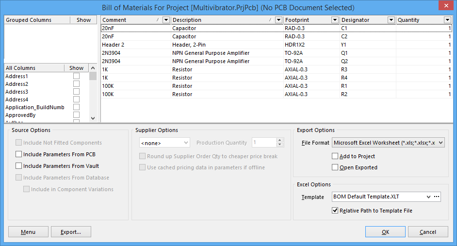
The report generation engine being used to generate a Bill of Materials.
- For more information about Report Outputs and configuring your Bill of Materials, see Report Outputs
- For more detailed information about generating a custom Bill of Materials, see Generating a Custom Bill of Materials.
Congratulations! You have completed the PCB design process.
Further Explorations
This tutorial has introduced you to just some of the powerful features of your Altium electronic design software. We've captured a schematic and designed and routed a PCB, but we've only just scratched the surface of the design power available to you. Once you start exploring, you will find a wealth of features to make your design life easier.
To demonstrate the capabilities of the software, a number of example files are included. You can open these examples in the normal way by selecting File » Open Project from the menus and then navigating to the Examples folder of your software installation.