Working with the Board Insight System
Contents
- Configuring the 2D Board Insight System
- Board Insight Lens
- Heads Up Display
- Board Insight Pop-up Mode
- Board Insight Panel Mode
- Visual Pick List
- Single Layer Mode
- Layer Transparency
- Active Layer Control
- Net Name Displayed on Tracks
- Net Highlighting
- Live Highlighting
- Pad and Via Detail Display Options
- Locked Objects Display Options
- 3D Board Insight
- Notes
- Displaying FPGA Information
Board Insight™ is a configurable system of features that give you complete control over viewing and working with your PCB design.
A complex multi-layer board makes for a visually dense and often difficult to interpret workspace. Altium Designer's Board Insight system makes it easier to view and understand the objects in your design. It consists of an integrated set of features developed to meet your view management needs.
2D Board Insight includes:
- Insight Lens
- Insight Panel
- Insight Pop-up
- Heads Up Display cursor information
- Floating graphical views
- Enhanced Single Layer mode
- Enhanced labeling on objects
Integrated with Board Insight are enhanced Single Layer mode and 3D visualization features. In Single Layer mode you can see clearly what is on a given layer, but also have perspective as to what is on other layers. With 3D visualization you can see a 3D model or cross-sectional views of your PCB, relevant to cursor position, in a separate panel.
Configuring the 2D Board Insight System

Press F2 to display the Board Insight pop-up menu.
2D Board Insight options are configured in the PCB Editor - Board Insight pages of the Preferences dialog. Here you can configure Board Insight options - from hover delays, lens shape and size, through to shortcuts. A quick way to access many of the Board Insight features, such as the Lens or Heads Up Display, is via shortcut keys. To help you learn the shortcuts, and as an alternate to remembering them, press F2 while you are working. This will open the Board Insight sub-menu (also accessible via the View menu), which you can use as a reference to read a shortcut from, or as a menu to select an entry.
Board Insight Lens
The Insight Lens makes light work of performing a detailed examination of your board. While the workspace remains at a low level of zoom you can closely inspect the smallest detail on the board, magnifying it in the Insight Lens. With its own zoom and single layer shortcuts, working with the Insight Lens will soon become second nature.
Use the Insight Lens to closely examine your board, here the Lens is showing a single layer view of the area highlighted in green.
Configure the size, shape and other Insight Lens properties in the PCB Editor - Board Insight Lens page of the Preferences dialog. It can be easier to work with the Insight Lens using the shortcut keys and mouse configuration settings, as detailed below:
| Shortcut | Function |
|---|---|
| SHIFT+M | Toggles the Insight Lens on or off. Use the lens when you need it. |
| SHIFT+N | Toggles the Insight Lens to move with the cursor, or drop it on the board at the current cursor location. Use this option to relocate the Insight Lens. |
| SHIFT+CTRL+M | Toggles the workspace zoom to display the contents of the Insight Lens. This allows you to see in more detail what is displayed in the Insight Lens. |
| SHIFT+CTRL+N | The Insight Lens moves with the cursor, centered around the cursor. |
| SHIFT+CTRL+S | Switches the Insight Lens into any of the available Single Layer modes (set in PCB Editor - Board Insight Display page of the Preferences dialog). The current layer objects are displayed in the lens, while all objects on other layers are masked or hidden, depending on the Single Layer mode being used. |
| F2 | Displays the Board Insight pop-up menu. |
| ALT+Wheel-roll | Changes zoom level inside the Insight Lens. |
| ALT+Wheel-click | Same as SHIFT + CTRL + M, toggles the workspace zoom to display the contents of the Insight Lens. |
Heads Up Display
the Board Insight Heads Up Display.
The Heads Up Display (HUD) gives you real-time feedback about objects currently under the cursor in the PCB workspace. The HUD is configurable, and can include cursor location, delta information (distance from the last mouse click), current layer and current-snap grid. As well as the information content, the display font and colors can also be configured. The HUD can be parked anywhere on the screen or you can have it follow the cursor, press the SHIFT + G shortcut to toggle between stationary and tracking modes.
| Shortcut | Function |
|---|---|
| SHIFT+H | Toggles the Heads Up Display on or off. Use this to decide when you want to use the display. |
| SHIFT+G | Toggles the location of the Heads Up Display to be at a fixed position on the board or allows it to be moved with the cursor. Use this option to move the Heads Up Display. |
| SHIFT+D | Toggles the display of the Delta Origin coordinates. The delta coordinates displays the distance, horizontally (dx) and vertically (dy), from the Delta origin coordinates. Use the Delta coordinates to gauge distance relative to a position on your board. |
| INS | Resets the Delta Origin to the current mouse coordinates. The distance horizontally and vertically the mouse is moved from the Delta Origin can be displayed in the Heads Up Display. This setting can be configured in the PCB Editor - Board Insight Modes page of the Preferences dialog. |
| F2 | Displays the Board Insight pop-up menu. |
Configure what information is displayed in the HUD in the PCB Editor - Board Insight Modes page of the Preferences dialog.
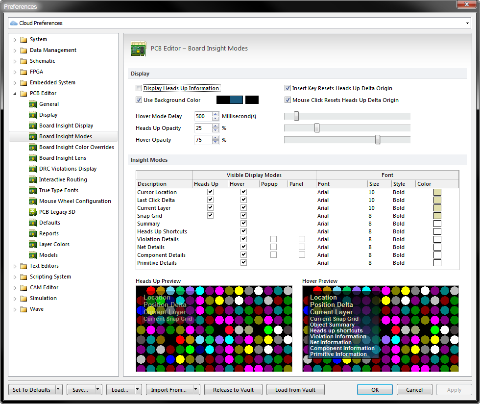
The PCB Board Insight Mode preferences.
In the Heads Up column of this dialog, enable each property option you want displayed. Font settings can also be adjusted.
Heads Up Display hover mode showing detailed information about objects currently under the cursor.
If you pause for a moment as you are moving the cursor, the Heads Up Display will switch to Hover mode. Extra information is displayed in Hover mode, this can include a summary, available shortcuts, rule violations, net, component and primitive details. Configure the HUD Hover mode in the PCB Editor - Board Insight Modes page of the Preferences dialog.
Board Insight Pop-up Mode
The Board Insight's Pop-up mode, being used to examine a design violation.
The Board Insight system's Pop-up mode is an excellent tool for interrogating objects under the cursor. Pressing SHIFT + X or SHIFT + V presents the Pop-up mode display, which includes list of all components, nets and violations under the cursor, and a graphical display of the object currently chosen in the list. From the list you can edit, select or zoom on any of the objects. As well as the component, net and violation group-type objects, the Board Insight popup list will include the primitive objects that were under the cursor and belong to them, such as pads and tracks. The list is hierarchical, allowing you, for example, to drill down for complete detail on the objects causing a violation.
Use the SHIFT + V shortcut to load the popup with information about violations currently under the cursor. SHIFT + X loads the popup with information about any nets and components under the cursor.
Board Insight Panel Mode
The Board Insight panel provides the same information as the popup view, in a panel, with no keystrokes required to update the contents (Figure 9). The panel allows you to view in more detail what is in under the cursor. When you hover the cursor over component, net or violation objects, they will be loaded into the panel. Once the information is in the panel it will remain until the cursor is paused in a new location.
The top region of the panel displays a graphical preview of the object.
The second region lists all primitives under the cursor. Here you can edit them, change their selection state and navigate to them. The available information can include listing components, nets and violations. From the list you can select, edit or zoom in on any of the objects.
The optional lower region of the panel (toggled via the Show Lens option) gives you a close up 2D view of the area currently under the cursor. There is also 3D Board Insight visualization available in the 3D Visualization panel, refer to the 3D Board Insight section of this article for more information.
The Board Insight panel works like any other panel - it can be resized, docked or floated over the workspace. The following table summarizes key shortcuts available when using the second (list) region of the panel:
| Shortcut / Icon | Function |
|---|---|
|
| Zoom into highlight item. The zoom level is controlled with by the Zoom Precision setting in the System - Navigation page of the Preferences dialog. |
|
| Click to toggle the selection state of one or more items. |
|
| Edit the item. |
| ALT+Wheel-roll | Changes zoom level inside the panel Insight Lens. |
| SHIFT+CTRL+S | Switches the Insight Lens into Single Layer mode. The current layer objects are displayed in the lens, while all objects on other layers are masked or hidden, depending on the Single Layer mode. |
| F2 | Displays the Board Insight sub-menu. |
The Board Insight panel gives detailed view of what is currently under the cursor.
Visual Pick List
The Visual Pick List makes it easy to choose the correct object in a crowded workspace.
A multi-layer PCB design makes for a dense and visually crowded workspace, with many objects on top of one another. The Visual Pick List pop-up makes object selection simple. When the mouse is clicked (or double-clicked) when there are multiple objects under the cursor, the Visual Pick List will appear. As you move the mouse through the list, the current object will be selected on the board, as well as be displayed in the popup, allowing easy identification. Objects in the Pick List are also sorted by layer.
Single Layer Mode
Integrated with Board Insight are the Single Layer mode features. Single Layer mode displays the contents of the current layer, hiding or dimming the contents of all other layers. As well as hiding all objects on all other layers to display only the contents of the current layer, Single Layer mode has two other display modes, allowing you to retain other layer data in your view, except displaying it without color. Converting all other layer colors to grayscale or monochrome lets you retain the spatial relationship information about the location of other objects in the design, without distracting you from the layer of interest. The background intensity and contrast for grayscale and monochrome modes is controlled using the Masked Objects Factor and Background Objects Factor slide controls from the Mask Level button at the bottom right of the PCB workspace.
Press SHIFT + S to cycle through the available Single Layer modes, which can include:
|
|
|
| Not in Single Layer Mode, displays all primitives on all layers. | Grayscale - primitives on other layers are displayed in grayscale shading. |
|
|
|
| Monochrome - primitives on other layers are displayed in the same shade of gray. | Hide Other Layers - primitives on other layers are not displayed. |
Single Layer mode behavior is configured in the PCB - Board Insight Display page of the Preferences dialog. By default, all three single layer display modes are enabled, meaning that you will cycle through them all as you press SHIFT + S. Use the checkboxes in this dialog to turn off any modes you do not want included when you press SHIFT + S. Mechanical layers also include an option to keep them displayed when Single Layer mode is enabled. The option is enabled in the View Configurations dialog (shortcut L).
Layer Transparency
The Board Insight system supports layer transparency. This feature allow you to see through objects to other objects underneath. To turn on layer transparency, enable the Use Transparent Layers option in the View Options tab of the View Configurations dialog. Note that the layers are drawn in the order defined in the Layer Drawing Order dialog (accessed via the PCB Editor - Display page of the Preferences dialog). For graphics cards that do not support DirectX 9 and Shader Model 3, requiring Altium Designer to use the GDI display mode, enable the Use Alpha Blending option to display moving objects correctly in Transparent mode (PCB Editor - Display page of the Preferences dialog).
Transparent layers let you see though objects to the objects below.
Active Layer Control
The PCB Editor is a multilayer environment, with one layer being currently active. As well as clicking on the Layer tab at the bottom of the workspace to make another layer active, you can move through the active layers by holding CTRL + SHIFT while rolling the mouse-wheel. Note that current layer selection applies only to the 2D editing mode.
Layer change shortcuts include:
| Shortcut | Function |
|---|---|
| CTRL+SHIFT+Mouse-wheel | Next layer / previous layer |
| + (numeric keypad plus) | Next layer |
| - (numeric keypad minus) | Previous layer |
| * (numeric keypad multiply) | Next signal layer |
Net Name Displayed on Tracks
Another handy feature to help you work more efficiently is the ability to display net names on the tracks (configured in the View Options tab of the View Configurations dialog). This option can be configured to display the net name once per track segment, or to repeat the name at regular intervals. Wherever you are working on the board, you can instantly be sure if the routing you are looking at is the net you are interested in. Regardless of whether or not you are showing net names on tracks in the main design window, the Board Insight lens always shows net names.
Displaying net names on the tracks makes it easy to "read" the routing.
Net Highlighting
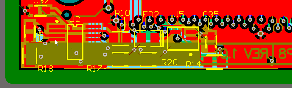
A modern PCB can be dense and difficult to interpret.
Making sense of a complex PCB design is not easy, with dense component placements, tight routing, and multiple signal layers. Altium Designer includes a number of net highlighting features to help you examine the routing. To highlight any net on the board, CTRL + Click on any net, and everything in the workspace that is not part of that net is faded, making the routing stand out on all signal layers, as shown in the figure below. To highlight multiple nets hold the SHIFT key as you CTRL + Click on each net. CTRL + Click in free space to restore the display, or click the Clear button at the bottom right of the workspace.
An example of a net being highlighted using CTRL + Click.
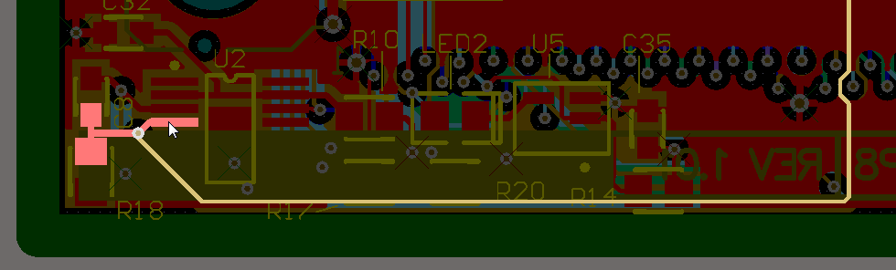
Live Highlighting
Net highlighting can be used dynamically too, meaning that as you move the cursor over a net, it can be highlighted. This method uses an outline highlight, which is configurable, and does not affect the display of the remainder of the PCB. The figure below shows the same net highlighted using Altium Designer's Live Highlighting.
An example of a net being highlighted using Live Highlighting.
|
Live Highlighting configuration options.
The PCB Editor - Board Insight Display page of the Preferences dialog has controls in the Live Highlighting region to enable and configure this feature. When enabled, this feature can be limited to highlighting only when the SHIFT key is pressed.
Pad and Via Detail Display Options
Pad and Via Detail Options.
You can control the display of pad and via details using the Pad and Via Display Options region of the PCB Editor - Board Insight Display page of the Preferences dialog, as shown above. Here you can configure font, color and background for pad and via information. Strings are automatically presented as right-reading, and aligned in the direction that maximizes the area available to display them. The Smart Display Color option automatically selects a font color to give good contrast so the text can be easily read.
Note: Depending on the display mode (DirectX or GDI), not all pad and via detail features will be visible.
Locked Objects Display Options
Locked objects can be highlighted by the Locked Object Texture.
Control when the display of locked objects occurs.
You can control how locked objects are displayed in the workspace, making them easier to identify visually. Use the controls in the Show Locked Texture on Objects region of the PCB Editor - Board Insight Display page of the Preferences dialog.
Note: The Locked Object texture is available in DirectX mode only. Object locking is available using the object's properties.
3D Board Insight
Related article: PCB 3D Projection Modes
Use the 3D mode to display the loaded board as if it were assembled.
Altium Designer's ability to display the board in 3D greatly enhances your ability to visualize the board as a manufactured and assembled object. Switch between 2D Layout Mode and 3D Layout Mode using the commands in the View menu, or the 2 and 3 shortcut keys.
The 3D Layout mode supports Orthographic and Perspective projection, press L when in 3D mode to open the View Configuration dialog and change the current Perspective setting. To learn more, read the PCB 3D Projection Modes article.
There are also a number of Board Insight features that use the 3D mode.
The 3D Visualization Panel displays the board in 3D, as well as 2 cross sections of the board.
The 3D Visualization panel displays up to three simultaneous 3D views, including 2 cross-sectional views and a 3D board view, as shown in the figure above. Using this panel you can examine all aspects of your board in 3D, including internal structures, whilst still working on the board in either 2D or 3D mode in the main PCB Editor window. Open the panel by selecting View » Workspace Panels » PCB » 3D Visualization, or by selecting 3D Visualization from the PCB button at the bottom right of Altium Designer.
The contents of the 3D Visualization panel displays are based on the position of the cursor in the main PCB Editor window. You can freeze or unfreeze the position of the 3D Visualization panel displays whilst moving around in the PCB Editor window by pressing SHIFT+F3. To alter the zoom or orientation of one of the views in the 3D Visualization panel, use the Left Drag to rotate view and Right Drag to zoom view shortcuts (click on the actual view in the 3D Visualization window to do this).
Use the ![]() controls to show/hide the various regions of the panel.
controls to show/hide the various regions of the panel.
|
|
|
| Relative position in 2D PCB Editor window. | Relative position in 3D PCB Editor window. |
The Configuration region of the panel allows you to select from any saved 3D view configuration (set in View Configurations dialog [shortcut L ]), which will control colours and surface opacity. The Thickness Scaling slide control alters the vertical scale of the board to make it easier to differentiate layers when viewing the PCB internally. You can select between 1 and 100 times the vertical scaling. The other controls relate to the cross-sectional views.
- The Section A-A region displays the Section A-A (X-axis) view.
- The Section B-B section displays the Section B-B (Y-axis) view.
- The 3D Board Insight region displays the fully floating 3D Board Insight perspective. You can zoom the view by left-dragging the mouse. You can zoom in to penetrate the PCB surfaces and even travel through the PCB internals. Right-drag the mouse to rotate the view in any direction. Rotation is about the current cursor position in the PCB Editor window.
Notes
- You need to have DirectX 9.0c or later installed and enabled in order to use the 3D display modes, including the 3D Visualization panel. Your graphics card must also support Shader Model 3. To enable DirectX in Altium Designer, open the PCB Editor - Display page of the Preferences dialog (DXP»Preferences). Enable the Use DirectX if possible option under Display Options in the right panel.
- With DirectX enabled, the Board Insight Lens shapes are always rectangular.
- You may notice that when traveling inside the PCB in the 3D Board Insight display that you can still be inside the board whilst your cursor is off the board in the PCB Editor window. This can occur because of the differing perspective, 3D positioning and zoom levels between the 3D Board Insight and the PCB Editor window views.
- The cursor position is not shown internally to the PCB in the 3D Board Insight display, however, is always the position from where the internal PCB perspective is based.
Displaying FPGA Information
To help the designer more intuitively manage programmable devices during the design process, the Board Insight System has been expanded to highlight FPGA component pins and connected routing, based on a user-selectable pin-type property.
FPGA pins and connected routing can be colored according to associated FPGA component information.
Altium Designer stores valuable FPGA component data which is used during the FPGA and PCB design processes. This information includes I/O bank allocations, I/O pins, clock pins, and differential pair pins. By selecting the appropriate Color Overlay mode in the PCB Component properties dialog, the component's pads and some of the connected routing will be highlighted in a range of colors, as shown in the figure above.
Double-click on a component on the board to set the *Color Overlay* mode.
Altium Designer's component libraries are already setup to use this information, the FPGA component detail is looked up in a database based on the component library name, for example XC3S1500-4FG676C. For new components, the part can either be named in the same manner, or a parameter called NexusDeviceID can be added to the schematic component, with the same data. Altium Designer will then be able to look up the new component in its database of FPGA parts.