Preparing the Board for Design Transfer
Contents
- Creating and Modifying the Board Shape
- Importing an Outline to Use for the Board Shape
- Defining the Board Shape From Selected Objects
- Defining the Board Shape from a 3D Body
- Modifying or Redefining the Board Shape
- Redefining the Board Shape Using Jump Location
- Using PCB Sheets
- Controlling the Display of the Sheet
- Keepouts
- Defining an All-layer Keepout
- Defining a Layer-specific Keepout
- Setting Up the PCB Workspace
- Grids
- Configuring the Mechanical and other Non-electrical Layers
- 2D Layout Mode
- 3D Layout Mode
- Setting up Design Rules
- Other Important Points about Design Rules
- Ready to Transfer the Schematic Design to the PCB?
This article describes how to prepare the new PCB file so that it is ready to transfer the design from the schematic editor. This includes defining the Board Shape, configuring the drawing sheet, setting up the layers and defining any keepout requirements, and setting the grids.
Creating and Modifying the Board Shape
Main article: Board Shape
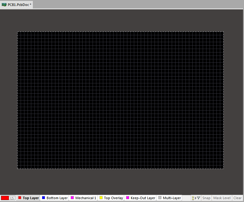
The default 6" by 4" board, with a 10 mil grid and a 10x Fine/Coarse grid display multiplier.
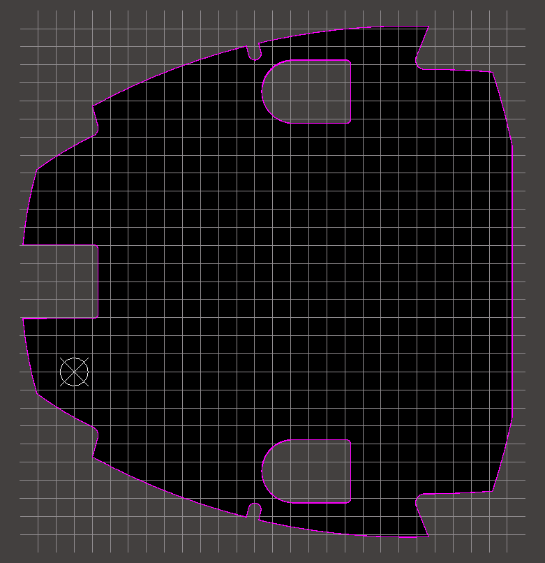
The Board Shape defines the boundary, or extents, of the board in the PCB Editor. The Board Shape is also referred to as the Board Outline, and is essentially a closed polygon. When you create a new PCB document, it is the black area with the visible grid showing inside (assuming the grid is coarse enough to see at the current zoom level).
The Board Shape is used by Altium Designer when:
- Splitting a board into multiple board regions,
- Placing bending line on a flex board region,
- Defining the extents of the power planes for plane edge pull back,
- Splitting power planes,
- Calculating the board edge when outputting design data to other tools.
When a new board file is created the default Board Shape is sized 6000 x 4000mil. The shape can be resized, or redefined, in a variety of ways. Note that PCB documents created using the PCB templates or the PCB Board Wizard have the Board Shape already correctly sized. Regardless of the final make up of the board (single rigid area or multiple rigid-flex sections), the overall outer shape is referred to as the Board Shape.
The Board Shape can be redefined:
- Manually - by redefining the shape, or moving the existing board vertices (corners). Switch to Board Planning Mode (View » Board Planning Mode) then use the commands in the Design menu.
- From selected objects - typically done from an outline on a mechanical layer. Use this option if an outline has been imported from an MCAD tool as a DWG/DXF file. Switch to 2D Layout Mode (View » 2D Layout Mode), select the primitives on the mechanical layer (Edit » Select » All on Layer), then use the Design » Board Shape » Define from Selected Objects command.
- From a 3D body - use this option if the blank board has been imported as a STEP model from an MCAD tool into an Altium Designer 3D Body Object (Place » 3D Body). Switch to 3D Layout Mode (View » 3D Layout Mode) then use the command in the Design » Board Shape sub-menu to select the Board Shape.
Importing an Outline to Use for the Board Shape
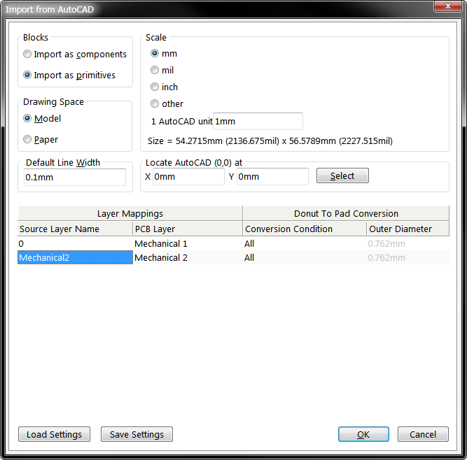
Ensure that the scale, default line width, and layer mappings are configured when importing DXF/DWG data.
You can set the Board Shape to match the shape defined by a set of objects on one of the PCB Editor's mechanical layers. Using this feature in combination with the ability to import DWG or DXF data from a mechanical CAD package, provides a method of transferring the Board Shape requirements from the mechanical CAD domain into Altium Designer.
To import a DXF/DWG file into a newly created PCB:
- Select File » New » PCB.
- The new blank PCB will open. The black region represents the current Board Shape. Before importing a new shape, set the following as required to suit the requirements of your design and the shape being imported:
- The Units - Design » Board Options
- The Grid - View » Grids » Grid Manager
- The Origin - Edit » Origin » Set, then click to define the location of the origin. It helps to set this to suit the location of the origin in the incoming outline.
- Now to import the board's shape as a .DXF or .DWG file. All versions of DXF/DWG date from AutoCAD 2.5 to 2013 are supported. Please note that the shape to be imported must be a closed shape, and internal cutouts are not automatically created (but can be defined later from imported objects).
- Select File » Import to open the Import File dialog, set the File Type down the bottom right of the dialog to AutoCAD (*.DXF,*DWG) and browse to find the required file.
- When the Open button is clicked the Import from AutoCAD dialog will open, as shown above.
- Set the Scale, Default Line Width and Layer Mappings as required, then click OK.
- Each DXF/DWG object will be mapped to an Altium Designer object, and displayed in the workspace. The image below shows a set of arc and line objects imported from a DWG file, which have been selected in Altium Designer.
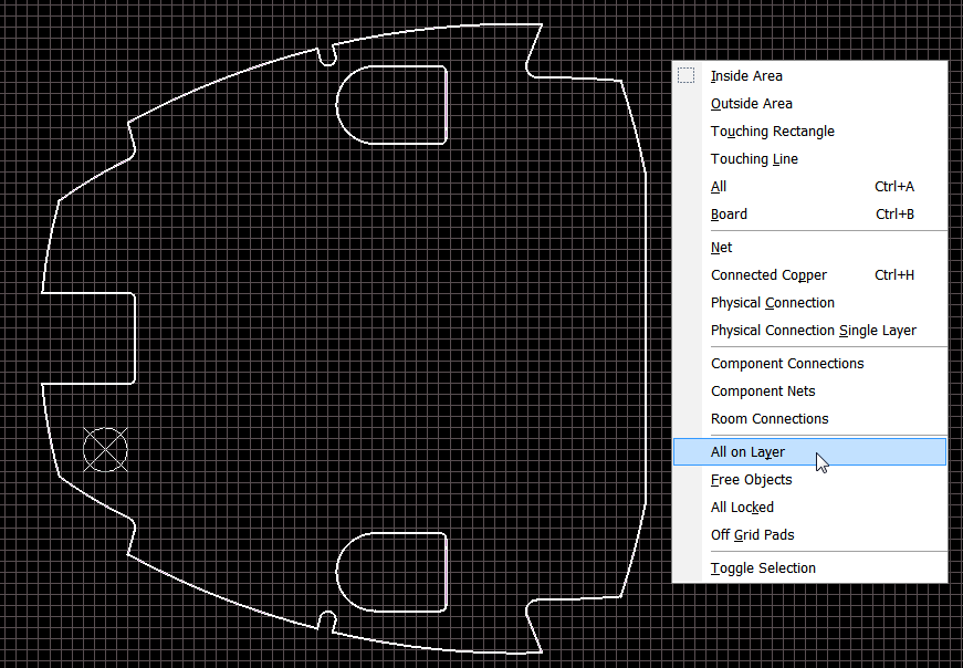
Imported arc and line objects, which are being selected.
There is now a closed boundary defined on a mechanical layer, which can be use to define the board shape.
Defining the Board Shape From Selected Objects
As mentioned, once an enclosed boundary of line and/or arc objects has been defined, these objects can be used to create the board shape, as shown in the image above.
To define a board shape from these objects:
- Set the View mode to 2D Layout Mode (View menu).
- Select the objects, the Edit » Select » All on Layer command is ideal for this, as shown in the image above.
- Run the Design » Board Shape » Define from selected objects command - the board shape will be redefined to the selected objects and the display updated.
Defining the Board Shape from a 3D Body
This feature redefines the board shape based on a surface (face) of an imported 3D STEP model. It can be used to quickly create a complex board shape and helps integration between electronic and mechanical design areas.This is a 2-stage process, first the STEP model is imported, then the required shape is selected from the STEP model.
To do this:
- Switch to View » 3D Layout Mode.
- To import the STEP model (.step or .stp) place a 3D body (Place » 3D Body), then in the 3D Body dialog enable the Generic STEP Model option, then use the Embed or Link buttons to import the required STEP model. Note that this STEP model can be deleted once the board shape has been redefined.
- Select Design » Board Shape » Define from 3D body.
- The Status bar will prompt to Pick a 3D body, click the imported 3D body to select it.
- The cursor will change to a crosshair and the Status bar will prompt Choose Face, as you hover the cursor over each face it will be outlined, click to select the correct face.
- The Board Outline Creation Successful dialog will appear, displaying options on how you want the imported 3D model positioned in relation to the newly defined board shape. These can be ignored if you are planning on deleting the STEP model, otherwise configure the options as required. Note that if you keep the STEP model embedded in or linked to the PCB file you will be notified whenever the STEP file changes. You will also be prompted to update the shape - a handy feature if the shape is still under development and updates are expected.
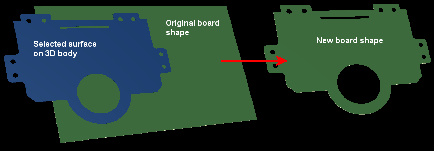
Defining the board shape from an imported STEP model.
Modifying or Redefining the Board Shape
In Board Planning Mode you can modify the board shape by moving the vertices, or completely redraw (redefine) it. Read the Board Shape article to learn more.
Redefining the Board Shape Using Jump Location
To accurately define the shape based on a set of dimensions, you can use the Jump Location shortcut keys instead of the mouse. To do this:
- Set the origin to define the location of the bottom left of the PCB (Edit » Origin » Set).
- Select Design » Board Shape » Redefine Board Shape and release the mouse.
- Press the J key to pop up the Jump submenu and then press the O key to jump to the origin you just defined. Press ENTER to define the first corner of the new board shape.
- Press J, L to display the Jump to Location dialog. The X-Location field will be active, so simply type in the X location of the next corner of the board (do not touch the mouse).
- Press the TAB key to move to the Y-Location field in the Jump to Location dialog and type in the appropriate Y value.
- Press ENTER to accept the values and close the dialog. The cursor will be at the correct location. Do not touch the mouse; simply press the ENTER key again to define this corner.
- Press J, L again to display the Jump to Location dialog, type in the next X coordinate, press TAB, type in the Y coordinate, press ENTER to accept the values and press ENTER to define this corner.
- Repeat this process until all corners are defined, finishing back at the 0, 0 origin. Again, do not touch the mouse; press ENTER.
Using PCB Sheets
The PCB Sheet is a special drawing feature used to represent the printed page in 2D Layout Mode. The sheet is not a design object, rather it is a display feature designed to work with objects placed on a mechanical layer. In the image below a grid reference has been drawn on Mechanical 16, and the sheet has been linked to this layer in the View Configurations dialog. Because it is linked and the Auto-size to linked layer option enabled (Board Options dialog), the Design » Board Shape » Autoposition Sheet command or the View » Fit Sheet command can be used to automatically resize the Sheet to exactly enclose the objects on that mechanical layer. This gives a professional, print-ready presentation of the board.
When you create a new PCB file, a default sheet is automatically created with the default size of 10000 x 8000mil. It is not shown initially, but when enabled in the Board Options dialog it appears as the white shape behind the design objects present in the workspace. Altium Designer's \Templates sub-folder includes a variety of template PCB files that include sheet borders for different paper sizes, open the appropriate sized template and copy the contents of the relevant mechanical layers into your current PCB design.
The sheet has been linked to the contents of Mechanical 16, resulting in a professional, print-ready presentation of the design.
As well as automatically defining the sheet size from the contents of the linked mechanical layers, the sheet size and location can be defined manually using the Sheet Position options in the Board Options dialog. Alternatively, if the contents of the linked mechanical layer change then use the View » Fit Sheet command or the Design » Board Shape » Auto-Position Sheet command to automatically resize the sheet to suit.

Control the display of the Sheet in the Board Options dialog.
Controlling the Display of the Sheet
To make the sheet visible in the PCB Editor:
- Select Design » Board Options to open the Board Options dialog, then enable the Display Sheet option in the Sheet Position section. The sheet can be hidden at any time by disabling the Display Sheet option. All linked mechanical layers will also be hidden.
- The color of the sheet can be changed in the View Configurations dialog (Design » Board Layers & Colors), select a new color for the Sheet Area Color and Sheet Line Color in the System Colors section of the dialog.
Keepouts
A keepout boundary defined from the board shape and the board cutouts.
As well as the board shape, you should also define a placement and routing boundary around the edge of the board. This is done by placing objects on the keepout layer. Objects placed on this layer define a no-crossing-allowed boundary for components and routing. Typically you want objects such as components and routing to be a certain distance from the edge of the board, this distance can be controlled by setting the applicable routing and component placement design rules. You can also define other routing and component keepouts areas for mechanical objects such as screw heads, or other mounting requirements.
Defining an All-layer Keepout
Keepout boundaries can be defined by placing any standard design objects: such as lines, arcs, fills and regions, on the Keepout layer. Objects placed on the Keepout layer create a keepout on all signal layers.
To define a keepout boundary, use one of the following methods:
- Manually place the required objects on the keepout layer.
- If the shape already exists on another layer, such as a mechanical layer, select the required objects using the appropriate command in the Select sub-menu, switch to the keepout layer, then use the Edit » Paste Special command to paste the clipboard contents onto the current layer.
- Create a keepout boundary that follows the board shape by running the Design » Board Shape » Create Primitives From Board Shape command (2D Layout Mode). The Line/Arc Primitives from Board Shape dialog will appear, set the keepout object Width and the Keepout Layer, then click OK to create the keepout boundary. Note the other options available in the dialog; the Include Cutouts option is ideal for creating keepouts around board cutouts (which can be important if there are polygons that must be poured around the cutout, and the Route Tool Outline option is handy when you need to define a mill-able rout path around the board. This is normally done on a mechanical layer, and by configuring this layer in the Route Tool Path option in the Board Options dialog, the routing slots can be displayed in 3D Layout mode.
Defining a Layer-specific Keepout
You can also define layer-specific keepouts on any copper layer. To do this:
- Click on the layer tab of the required layer.
- Define the boundary or area of the keepout area by placing layer-specific keepout objects (Place » Keepout submenu). Layer specific keepouts are simply standard objects with the Keepout attribute enabled. They are displayed in the same color as the layer, with a keepout colored edge. Note that layer-specific keepout objects are not included in the Gerber or ODB++ output files.
Setting Up the PCB Workspace
Now you have created the board shape, configured the sheet and defined the keepout boundaries, the next step is to set up the workspace, including: the grids, layers and design rules.
Grids
Related article: Grid Manager (PCB)
You need to ensure that a suitable grid is set defined before you start positioning any components on the board. Altium Designer supports any number of user-defined grids, in either Cartesian (rectangular) or polar (radial) form. Grids are defined in the Grid Manager and are prioritized, with the highest priority grid under the current cursor location being the current, or active grid. Grids can also be restricted to either apply to component objects only, or all other object kinds only.
Remember that since all objects placed in the PCB Editor workspace are aligned to the current or active grid, the grids should always be appropriately defined. For example, for routing the grid needs to be set to suit the routing technology (width/clearance) that you intend to use.

To define or modify a grid:
- Click the Snap button down the bottom right of the workspace (as shown in the image above), and select Grids from the menu to open the Grid Manager dialog.
- The default Global Board Snap Grid will be listed, double-click to configure it, or click the Menu button to add a new grid.
- To edit the current grid while working, press the Ctrl+G shortcuts.
- To learn more about related features, such as Guides and Object Snap behavior, refer to the article; Unified Cursor-Snap System (PCB).
Defining the Design Layers in the Layer Stack Manager
Related article: PCB Layer Stack Management
There are three types of layers in the PCB Editor:
- Electrical layers - These include the 32 signal layers and 32 plane layers. Electrical layers are added to and removed from the design in the Layer Stack Manager dialog (Design » Layer Stack Manager).
- Mechanical layers - There are 32 general purpose mechanical layers for defining the board outline, placing dimensions on, including fabrication details on, or any other mechanical details the design requires. These layers can be selectively included in print and Gerber output generation. You can add, remove and name mechanical layers in the View Configurations dialog. You can save any custom views you create as view configurations, which you can re-use time and again. Enable the Only show enabled mechanical layers option to limit the list to only enabled layers. Before a Mechanical layer can be used, it must be enabled. Enable the checkbox in the Enable column to specifically make that mechanical layer part of the current PCB design. To edit a mechanical layer name, click to select it, then press F2 to edit it. The Show option allows you to control the visibility of a mechanical layer. The Display In Single Layer Mode option causes that layer to be displayed when Single Layer Mode is used (use SHIFT+S to cycle it on and off). Enable the Linked To Sheet option to relate a mechanical layer to the PCB sheet object. Related linked mechanical layers are hidden when the Display Sheet option is disabled (Board Options dialog). They are also used to determine the extents of the sheet when the Auto-position sheet option is chosen in the Board Shape sub-menu.
- Special layers - These include the top and bottom silkscreen layers, the solder and paste mask layers, the Keep-Out layer (used to define the electrical boundaries), the multilayer (used for multilayer pads and vias), and the drill layers (Drill Guide and Drill Drawing).
- System layers - the connection layer, DRC error layer, grid layers, hole layers, and workspace layers. Technically these are not layers in the sense that design objects can not be placed on them, but it is easier to think of them as layers as their visibility and color is also controlled in the View Configurations dialog.
All of the design layers that are part of the fabrication process, including the: Copper layers; Mask/Coverlay layers; and Overlay layers, are configured in the Layer Stack Manager. As well as adding/removing layers, the Layer Stack Manager is also used to define extra layer stacks. This ability to define multiple stacks is a core requirement of Rigid-Flex design.
To add, edit or remove design fabrication layers:
- Select Design » Layer Stack Manager [shortcut: D, K] to display the Layer Stack Manager dialog.
- New layers can be added to the design as required, by selecting an existing layer and clicking the Add Layer button. New layers are added below the currently selected layer. Once the required layers have been added, use the Move Up and Move Down buttons to configure the layer stack.
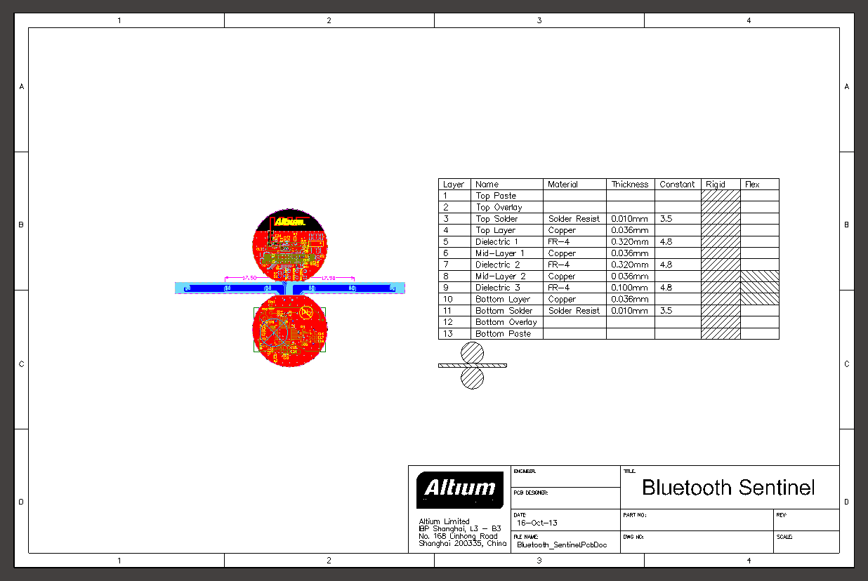
- To edit the properties of a layer, double-click on the appropriate cell to edit that cell. Layer properties, such as copper thickness and dielectric properties are used for signal integrity analysis, and are also included in the Layer Stack Table.
- The stack-up style refers to the order of the insulation layers through the layer stack. The list includes four stack-up styles - Layer Pairs, Internal Layer Pairs, Build-Up and Custom. Changing the layer stack-up style changes the way that the core and prepreg layers are distributed through the layer stack. Select the preferred stack-up style from the drop-down list located at the top-right of the dialog. Defining the stack-up style is important if you plan to use blind and buried vias, or perform a detailed signal integrity analysis of the design. If you require blind and buried vias, you must define the allowed drill pairs by clicking on the Drill Pairs button. Note that drill pairs must be defined for each of the defined layer stacks.
- Click OK to close the dialog.
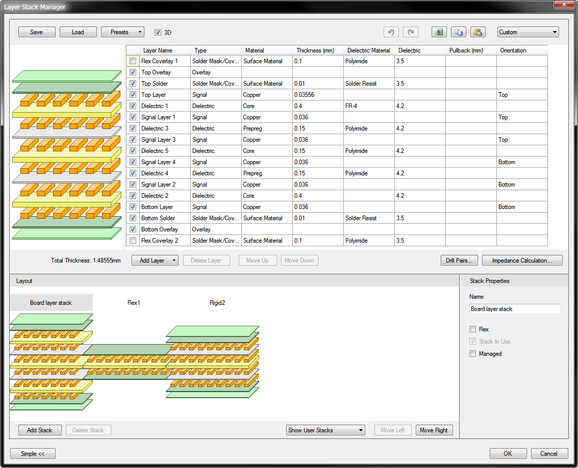
The Layer Stack Manager, showing the 3 stacks and the layers needed for a rigid-flex design.
Configuring the Mechanical and other Non-electrical Layers
All other layers are configured in the View Configurations dialog (Design » Board Layers and Colors, or press the L shortcut), as shown in the image below. Note that the presentation of the View Configurations dialog will change, depending on if the workspace is currently in 2D Layout Mode or 3D Layout Mode (View menu). In both modes there are 2 main regions in the dialog, the section on the left that is used for selecting, creating or configuring a View Configuration, and the section on the right where you configure the various display settings. A View Configuration is simply a snapshot of all the settings available on the right of the dialog, which you can configure, save and load as required.
2D Layout Mode
In 2D Layout Mode the main section on the right of the View Configurations dialog is used to configure and enable the special layers and the system layers. This section also includes tabs for: controlling the display state of each object type (Full, Draft or Hidden) on the Show/Hide tab; configuring various display options on the View Options tab; and configuring the transparency options in the Transparency tab. Note that there are also settings that effect the transparency of objects in the PCB Editor - Display page of the Preferences dialog.
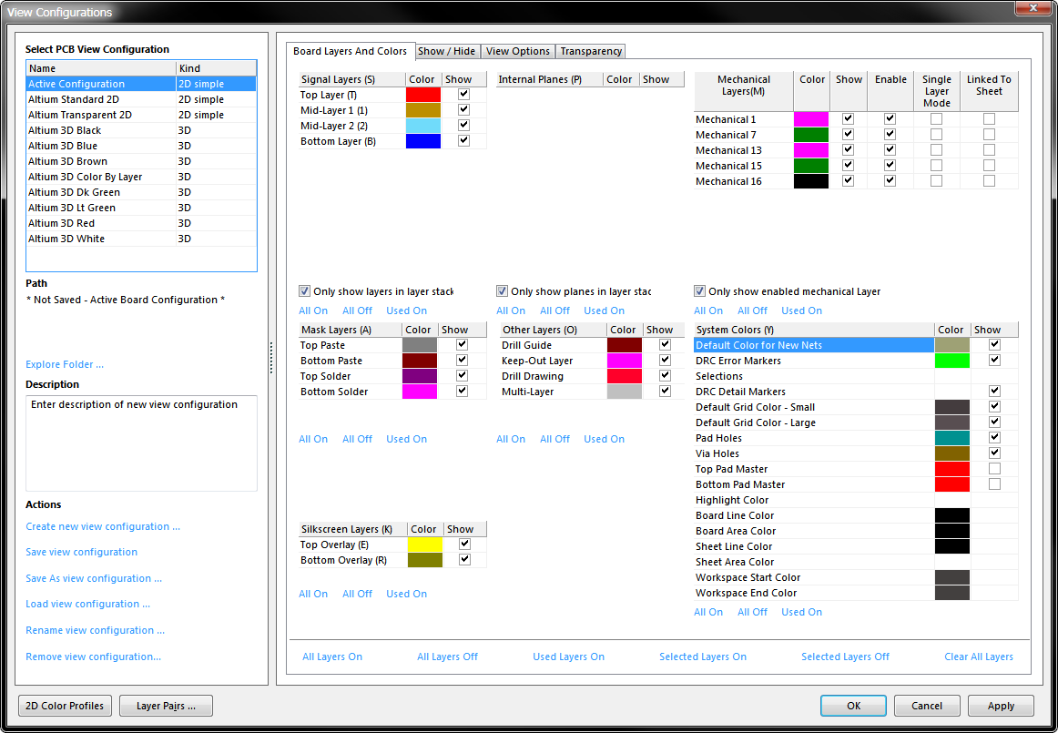
The View Configurations dialog when the design is being viewed in 2D Layout Mode.
3D Layout Mode
If the workspace is in 3D Layout Mode, the the View Configurations dialog will open as shown below. The right side of the dialog includes options for configuring how the board is rendered in 3D.
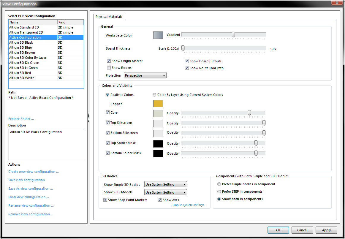
The View Configurations dialog when the design is being viewed in 3D Layout Mode.
Altium Designer's 3D Layout Mode displays the board as a realistic, 3 dimensional representation of the finished board. If the component footprints include 3D Body objects to represent the mounted components, then you will get an accurate representation of the finished board, with full support for 3 dimensional clearance checking. You can even import the product enclosure as a STEP file and check the board for fit. Add a 3D mouse, such as a SpaceNavigator to your PC, and you can view, rotate and examine the loaded board as if you were holding it in your hand.

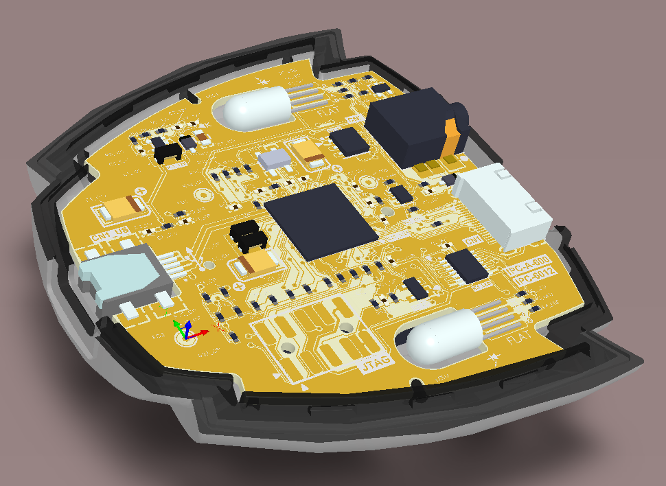
The same design shown in 2D and 3D Layout Modes. In 3D mode the board is sitting in the lower half of it's case.
Setting up Design Rules
Related article: Design Rules
The last step to preparing the empty PCB workspace is to configure the Design Rules. Altium Designer is a rules-driven design environment, with a flexible and powerful real-time design rule checking system. Rather than configuring design requirements on a primitive-to-primitive basis, you target the rules by writing a rule query, which specifies which objects that rule is to target. For example you might define routing widths for all nets in a net class, the paste mask requirements for a specific component, or which layers a specific set of nets must be routed on. Rules are also hierarchical, so you can define multiple rules, with higher priority rules overriding lower priority rules when appropriate.
Design rules are defined in the PCB Rules and Constraints Editor dialog (Design » Rules).
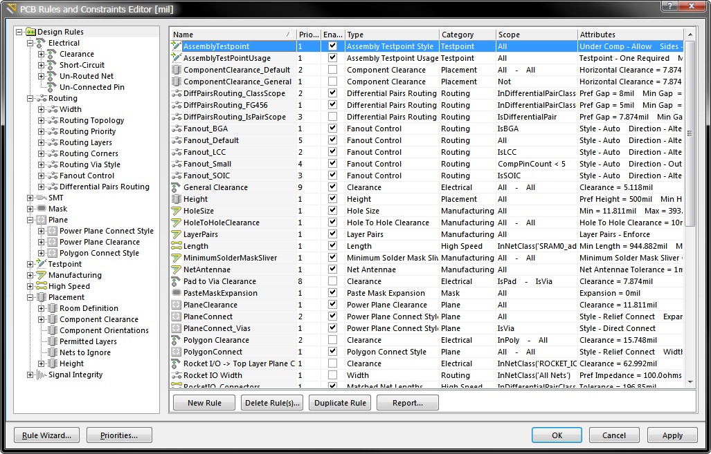
Create and configure the design requirements as design rules, here the dialog is displaying all rules defined for this board.
An example of a differential pair routing rule, scoped to target All Differential Pairs that touch a specific room. This rule sets the width/clearance under a BGA to be narrower/closer than the width/clearance on the rest of the board, which is specified in a lower priority rule.
Other Important Points about Design Rules
- As well as manually defining a rule from scratch, you can also use the Design Rule Wizard (Design » Rule Wizard) to help you create the rule. You can also use the Query Builder, you'll find a button to open it in the query definition region of each design rule.
- There is great value in creating the design rules as early as possible, not only will the online DRC (configured in Tools » Design Rules Check) immediately flag violations as soon as they occur, in many situations you will be prevented from creating violations in the first place.
- If you have created a set of design rules that can be reused in other projects, right-click in the Design Rule tree on the left of the PCB Rules and Constraints Editor dialog to export/import rules.
- For more information about setting up the design rules, refer to the article Creating Design Rules. To understand more about design rule violations, refer to Interrogating Violations.
Ready to Transfer the Schematic Design to the PCB?
Before transferring the schematic information from a schematic document to the new PCB, make sure:
- Your PCB file is part of the same .PrjPCB project as the schematics.
- That all the libraries that include the required PCB footprints are available. For more information about using libraries, refer to Component, Model and Library Concepts.
- The project has been compiled (Project » Compile Project) in the Schematic Editor, and that any errors in the schematic have been corrected.
To transfer the design from the schematic to the PCB, run the Design » Update PCB Document command. This will generate a set of ECOs that will transfer the schematic information to the target PCB. For more information about updating a PCB, refer to the Tutorial - Getting Started with PCB Design.