Signal Integrity
Contents
Parent page: SignalIntegrity((Panels))
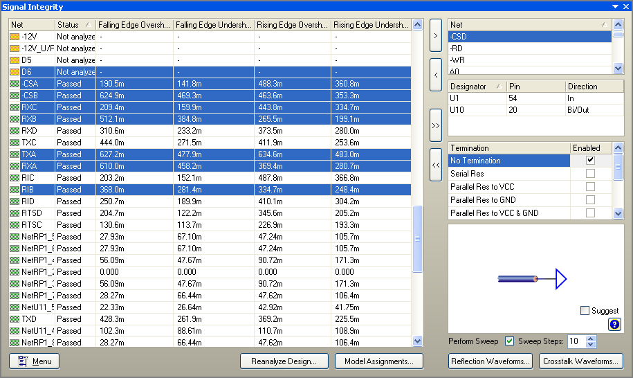
The Signal Integrity panel is used to configure and control the signal integrity analysis process.
Summary
The Signal Integrity panel is the control center for performing signal integrity analysis on a design. It enables you to screen all nets in a design, against various defined signal integrity rules, in order to quickly identify problematic nets. These nets can then be analyzed in greater detail by running fast reflection and crosstalk analyses. The ability to add virtual terminations allows you to ascertain what additional circuitry need be added to the design to resolve these problem areas and hence obtain the most efficient signal integrity performance.
Panel Access
The Signal Integrity panel is only available after a signal integrity analysis has been performed. Select Tools » Signal Integrity from the schematic or PCB editor menus to perform a signal integrity analysis on the current design. Once an analysis has been performed, click the ![]() button at the bottom-right of Altium Designer to display the panel. Alternatively, you can access the panel through the View » Workspace Panels » Editor » Signal Integrity sub-menu entry.
button at the bottom-right of Altium Designer to display the panel. Alternatively, you can access the panel through the View » Workspace Panels » Editor » Signal Integrity sub-menu entry.

Use the Signal Integrity button to access the panel once a Signal Integrity analysis has been performed.
Screening Analysis
The left-hand side of the panel provides the results from screening analysis of the current design. The first time a signal integrity analysis is run for a design a default screening analysis will be performed, using default overshoot/undershoot tolerances and any user-defined signal integrity design rules.
The screening results are listed in tabular format. For each net in the design the following column information can be displayed:
| Net | The net name and a graphical representation of its status. This column is permanently displayed. |
| Status | A textual representation of the net's screening analysis status. This column is displayed by default. |
| Analysis Errors | Information as to why a net can't be analyzed. |
| Base Value | The voltage that the signal on the net settles to in the low state. |
| Falling Edge Flight Time | The time it takes for the signal on the net to fall to the threshold voltage, less the time it would take for a reference load (connected directly to the output) to fall to the threshold voltage. |
| Falling Edge Overshoot | The maximum overshoot (ringing below the base value) on the falling edge of the signal. This column is displayed by default. |
| Falling Edge Slope | The time it takes for the signal on the net to fall from the threshold voltage (VT), to a valid low (VIL). |
| Falling Edge Undershoot | The maximum undershoot (ringing above the base value) on the falling edge of the signal. This column is displayed by default. |
| Length | The total net length (sum of all routed track segments in the net). |
| Impedance | The average impedance for the net (in Ohms). This is the average of the impedance of each track segment, weighted by its length. |
| Rising Edge Flight Time | The time it takes to drive the signal on the net to the threshold voltage, less the time it would take to drive a reference load (connected directly to the output) to the threshold voltage. |
| Rising Edge Overshoot | The maximum overshoot (ringing above the top value) on the rising edge of the signal. This column is displayed by default. |
| Rising Edge Slope | The time it takes for the signal on the net to rise from the threshold voltage (VT), to a valid high (VIH). |
| Rising Edge Undershoot | The maximum undershoot (ringing below the top value) on the rising edge of the signal. This column is displayed by default. |
| Routed | Shows whether the net is routed (full or partial) in the design (True) or totally unrouted (False). |
| Top Value | The voltage that the signal on the net settles to in the high state. |
Use the Menu button or right-click in the table to access the Show/Hide Columns sub-menu, from where you can enable/disable the display of data columns as required.
Each net in the design is assigned one of three possible status settings:
|
| Passed - all values within specified tolerance level for each of the defined rules. |
|
| Failed - At least one value outside specified tolerance level for one or more of the defined rules (entry associated with violated rule is shaded pale red in color). |
|
| Not Analyzed - Net unable to be screened. |
Notes about the presentation in the Panel:
- Any nets containing other errors that will lead to incorrect results in both screening and further analyses, will appear with their entire row entry colored in bright red.
- Any nets that are totally unrouted in the PCB will appear with their entire row entry colored in light grey.
- Use the main screening analysis area of the panel to quickly identify problem nets in the design. These nets can then be investigated in greater depth using the Reflection and Crosstalk analyses.
Menu Button
Click the Menu button at the bottom left of the panel to access the following commands. Note that these commands are also available via the right-click menu, anywhere in the screening results table:
- Details - this command is only available when a single net is selected in the screening results table. It is used to open the Full Results dialog, containing all of the screening analysis results that can be displayed in the results table, along with the following:
- Component Count - how many components have pads that connect to the selected net
- Track Count - how many individual routed track segments comprise the total routed net
- Minimum Impedance (Ohms) - the minimum impedance for the net, considering the individual impedances of all track segments in the net
- Maximum Impedance (Ohms) - the maximum impedance for the net, considering the individual impedances of all track segments in the net.
- Find Coupled Nets - this command enables you to quickly identify which nets are considered to be coupled to the selected net(s) you choose in the screening analysis results area of the panel, based on coupling criteria specified in the Configuration tab of the Signal Integrity Preferences dialog (accessed through the Preferences command on the menu). All coupled nets will become selected in the table. This feature is very useful when you want to determine which nets might suffer from crosstalk and allows you to quickly select them for use in a crosstalk analysis.
- Cross Probe - this entry of the menu leads to a sub-menu, from where you can cross probe to the selected net(s) on either a source schematic document or the PCB document. The target document will be made active in the design editor window and the selected net(s) will be displayed in accordance with the highlighting methods defined on the System - Navigation page of the Preferences dialog (DXP » Preferences)
- Copy - this menu entry leads to a sub-menu from where you can choose to copy all of the currently displayed screening analysis information, or information for selected nets only. The copied information is placed on the standard Windows clipboard, from where it can be pasted into other applications for further use
- Show/Hide Columns - this entry leads to a sub-menu listing all of the data columns that can be displayed in the screening analysis results area of the panel. Enable/disable the display of information as required. Currently displayed data columns are indicated with a tick symbol to the left of the entry. By default the data is sorted using the Status column and in ascending order. To sort by another column, click on the header for that column. Clicking repeatedly on a column header will toggle between ascending and descending sort order.
- Preferences - this command is used to open the Signal Integrity Preferences dialog, from where you can define various settings to be applied to all signal integrity analyses performed. These settings include the integration method to be used and accuracy thresholds to be applied.
- Set Tolerances - this command is used to open the Set Screening Analysis Tolerances dialog. This dialog lists four default overshoot/undershoot rules and any signal integrity design rules that have been defined (in either the schematic or PCB). From this dialog you can control which rules are enabled when performing a screening analysis of the nets in the current design. The four default rules can be edited in-situ, but any defined signal integrity rules must be edited from the PCB Rules and Constraints Editor dialog (an access button for which, is provided).
- Display Report - this command is used to generate a signal integrity report (Signal Integrity Tests Report.txt). The report is generated in the same location as the parent design project file, added to the Projects panel under the Generated\Text Documents sub-folder and opened as the active document in the design editor window. The report lists, for each enabled rule, which nets failed the rule and also which nets could not be analyzed.
Reanalyze Design Button
The Reanalyze Design button allows you to perform the screening analysis again for the current design and should be used if you have made any changes to the design documents. In this way, you are assured of having the most up-to-date results for your design. You do not need to reanalyze the design after adding/editing signal integrity design rules as the screening results are compared against the enabled rule tolerances in real time.
Model Assignments Button
Each component in the net under test must have a suitable Signal Integrity model assigned. Use the Model Assignments button to open the Signal Integrity Model Assignments dialog:
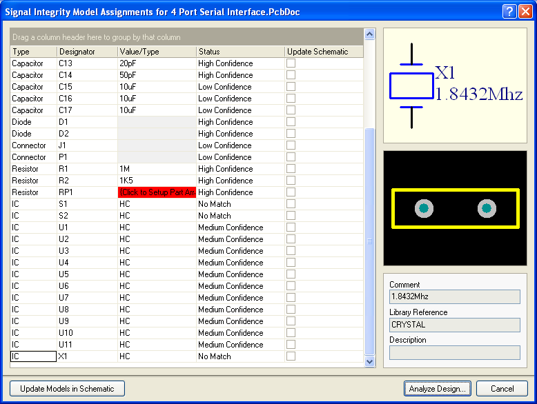
This dialog lists all components in the current design and, for each, attempts to make an educated guess as to the necessary signal integrity model required if one has not already been defined and linked. It is important to assign models as accurately as possible in order to achieve optimal signal integrity analysis results for your design.
Reflection and Crosstalk Analyses
The top-right section of the panel (Net) displays a list of all nets that have been taken across for further, detailed analysis (reflection or crosstalk).
Nets can be added to/removed from this section by using the available arrow buttons. Alternatively, double-click on a net in the screening analysis results area of the panel to add it to the Net section, or double-click on a net entry in the Net section to remove it. The panel sections below the list of Nets display information about the net that is currently selected.
Right-click on an entry in the list to access a pop-up menu providing the following commands:
- Clear Status - use this command to clear the assigned Aggressor/Victim states of all nets in the list.
- Set Aggressor - use this command to set the chosen net to be the Aggressor net when performing a crosstalk analysis. All other nets in the list will automatically be set to Victim status.
- Set Victim - use this command to set the chosen net to be the Victim net when performing a crosstalk analysis. All other nets in the list will automatically be set to Aggressor status.
- Cross Probe - this entry of the menu leads to a sub-menu, from where you can cross probe to the selected net(s) on either a source schematic document or the PCB document. The target document will be made active in the design editor window and the selected net(s) will be displayed in accordance with the highlighting methods defined on the System - Navigation page of the Preferences dialog (DXP » Preferences).
As you click on a net in the Net section of the panel, the section immediately below will display all component pins that are attached to that net. Depending on the type of pin, the following commands will be available from the right-click menu:
- Toggle In/Out - available for bidirectional pins only. Allows you to toggle the direction of the pin
- Edit Buffer - opens the relevant data dialog for the pins' associated component, allowing you to edit various properties specific to the component type (e.g. part technology and pin models for an IC, cable and termination for a Connector, etc.)
- Cross Probe - allows you to cross probe to the pin/pad on the schematic or PCB document respectively. The target document will be made active in the design editor window and the selected pin/pad will be displayed in accordance with the highlighting methods defined on the System - Navigation page of the Preferences dialog (DXP » Preferences)
Termination Advisor
The lower-right section of the panel gives access to the Termination Advisor.
Eight termination types are provided, with No Termination enabled by default. As you click on a termination type, a graphical representation is displayed in the window below. Multiple termination types can be enabled when performing reflection and crosstalk analyses - a separate set of waveforms will be produced for each. This allows you to determine the best termination to add to the design to achieve optimal signal quality on transmission lines and therefore reduce reflections (ringing) to an acceptable level.
Click on the help symbol icon to pop-up information about the termination. Fields for Min and Max termination component values are also displayed. You can either enter your own values for the termination components, or enable the Suggest option. In this case, values will be calculated based on your design and relevant formulae for the termination type. The values will be entered and become non-editable.
Selecting to use a termination adds a virtual termination to the design, just for analysis purposes. This allows you to test various termination strategies without physically altering your design. When the Serial Res termination is enabled, it is added to all output pins in the net listed in the Net section of the panel. For all other termination types, the termination is added to each input pin in the net.
Use the Reflections and Crosstalk buttons as required to proceed with running an analysis. Enable the Perform Sweep option if you want to run the analysis with a swept range of values for the termination components. The values used at each sweep of the analysis will depend on the minimum and maximum values entered and the value chosen in the Sweep Steps field (e.g. a if Sweep Steps is set to 2, the first pass of the analysis will use the minimum value and the second the maximum).
Waveforms
As an analysis proceeds, a simulation data file (ProjectName.sdf) is generated. The file is added to the Project under the Generated\Simulation Documents sub-folder and opens as the active document in the design editor window, displaying the results of analysis in the Simulation Data Editors Waveform Analysis window.
Each net included in a reflection analysis will have its results displayed in its own chart, identified as a separate tab with the net name at the bottom of the Waveform Analysis window. Each chart will contain wave plots for each pin in the net and for each enabled termination type. Waveforms for each sweep (if enabled) will appear in each plot, along with the waveform for No Termination.
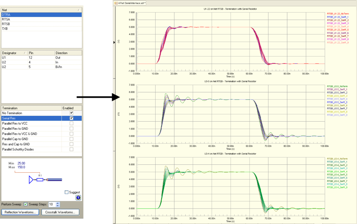
The net under test has 3 pins, resulting in 3 plots in this reflection chart. Each plot displays a number of waveforms, one for each sweep of the termination as well as a no termination sweep.
When a crosstalk analysis is performed, a single chart of results will be generated (identified as the Crosstalk Analysis tab). The chart will contain wave plots for each pin in each net and for each termination type enabled. Again, waveforms for each sweep (if enabled) will appear in each plot, along with the waveform for No Termination. Click on a sweep label on the right of the waveforms to examine the termination component values used for that sweep.
Having run detailed analyses and identified the optimal termination to add to the design, right-click on the termination entry in the panel and choose the Place On Schematic command. The Place Termination dialog will appear:
Use the dialog to choose which component(s) to use (in which libraries), whether to use automatic or manual placement, whether to place on all applicable pins or just the selected pin and the exact values to be used for the component(s).
When placing termination components, the Signal Integrity Analyzer will automatically identify the source schematic document that the pin(s) belong to and make this the active document in the design editor window. If you have selected automatic placement, the component(s) will be placed at the bottom left corner of the document. Place and connect as required. You will need to synchronize the schematic with the PCB to pass on the changes to the board design.
Notes
- In order to run a successful signal integrity analysis of the design and obtain accurate results, the associated signal integrity model type for each component has to be correct. This is achieved by setting the correct entry for the Type field in the Signal Integrity Model dialog, when editing the SI model associated to the component placed on the schematic source document. Alternatively, set the correct type from the Signal Integrity Model Assignments dialog. If this entry is not defined, the type Integrated Circuit will be assumed.
- Although each net can be screened to provide net and impedance data, not all nets can be analyzed for signal integrity characteristics (voltage and timing). In order to screen successfully for all characteristics, a net must contain at least one IC with an output pin and no other components. Resistors, capacitors and inductors will not simulate for example, because of their lack of output pin to provide a driving source. It should be noted that when bidirectional nets are screened, both directions are simulated and the worst case result is displayed.
- Any signal integrity-related warnings and errors will appear in the Messages panel when the screening analysis is performed. If a net entry in the screening results region of the Signal Integrity panel is highlighted in bright red, double-clicking on it will open the Errors Detected dialog with more detail as to why the net could not be analyzed. The same message will be added to the Messages panel, from where you can then cross probe in order to resolve the issue in the source document.
- Default overshoot and undershoot tests are defined as these are probably the best characteristics to use in determining which nets may be the most problematic.
- Any number of nets can be taken across to the Net section of the panel for further analysis. If running a reflection analysis, try to keep the quantity of nets to a manageable level, as analysis time increases considerably when a larger numbers of nets are involved. If running a crosstalk analysis, the typical number of nets taken across would be three - a net and its two immediate neighbors.
- For reflection analyses, the Signal Integrity Analyzer calculates voltages at nodes of a net using routing and layer information from the PCB and associated driver and receiver I/O buffer models. A 2D-field solver automatically calculates the electrical characterization of the transmission lines. Modeling assumes that DC path losses are small enough to be ignored.
- The level of crosstalk (or the extent of EMI) is directly proportional to the reflections on a signal line. If the signal quality conditions are achieved and reflections are brought down to a near-negligible level through correct signal termination, i.e. the signal is delivered to its destination with minimal signal stray, crosstalk will also be minimized.
- As you run subsequent reflection and crosstalk analyses on different nets, the results will be added to the same simulation data file, appearing as new charts (tabs at the bottom of the Waveform Analysis window).
- The filtering applied when cross-probing from the Signal Integrity panel to a schematic source document is temporary. Clicking inside the design editor window will clear the filter. As such, you are not prevented from selecting or editing design objects that fall outside the scope of the filter. If the Masking highlight method has been enabled, the extent of masking can be manually adjusted using the Dim slider bar - accessed by clicking the Mask Level button, to the immediate left of the Clear button, at the bottom-right of the design editor window.
- The filtering applied when cross-probing from the Signal Integrity panel to a PCB document is permanent. If the Masking highlight method has been enabled, all objects not falling under the scope of the filter will become faded in the workspace and are not available for selection or editing. The extent of the masking is controlled by the Mask slider bar, again accessed by clicking the Mask Level button. Clicking inside the design editor window will not clear the filter. A permanent filter must be cleared by clicking on a corresponding Clear button (e.g. at the bottom-right of the design editor window or from within the PCB panel).
-
All output files will be stored at the same location as the parent project document.