Defining & Running Circuit Simulation Analyses
Contents
- Creating a New Project
- Creating a New Schematic Sheet
- Drawing the Schematic
- Locating Components and Loading Libraries
- Placing a Simulation-ready Component
- Adding a New SIM Model File
- Adding the Simulation-ready Resistors
- Setting Up Simulation-ready Capacitors
- Adding the Voltage Sources
- Wiring Up the Circuit
- Adding Power Ports
- Compiling the Project
- Setting Up the Analyses
- Setting Up a Transient/Fourier Analysis
- Setting Up an AC Small Signal Analysis
- Running the Simulation
- Creating a Bode Plot
- Using the Measurement Cursors
- Running a Parameter Sweep Analysis
- Using a SPICE Netlist for Simulation
This tutorial takes you through the process of creating a simulation-ready schematic, which is then used to run a number of circuit simulation analyses. We will start by creating a new project file and then add a blank schematic sheet.
Creating a New Project

To start the tutorial, create a new PCB project:
- Select File » New » Project » PCB Project from the menus.
- The Projects panel displays. The new project file,
PCB Project1.PrjPCB, is listed, with no documents added. - Save and rename the new project file by selecting File » Save Project As. Navigate to a suitable location, type the name
Filter.PrjPCBin the File Name field, and click on Save.
Next, we will create a new schematic sheet to add to the empty project file. This schematic will be for a Filter circuit. If you do not have the time to draw the schematic from scratch, you can download a similar project Filter.PrjPCB from the Download Examples and Reference Designs page.
Creating a New Schematic Sheet
Create a new schematic sheet by completing the following steps:
- Select File » New » Schematic. A blank schematic sheet named Sheet1.SchDoc displays in the design window of the Schematic Editor and the schematic sheet is now listed under Source Documents beneath the project name in the Projects panel.
- Rename the new schematic file (with a
.SchDocextension) by selecting File » Save As. Navigate to a location where you would like to store the schematic on your hard disk, type the nameFilter.SchDocin the File Name field and click on Save.
Drawing the Schematic
Now we can create the Filter circuit shown below. Before we can run a simulation, the schematic must contain components with SIM models attached, voltage sources to power the filter, an excitation source, a ground reference for the simulations and some net labels on the points of the circuit where we wish to view waveforms.
In this section of the tutorial, we will locate the components required, set up their component properties and then wire the schematic.
Schematic of the Filter circuit.
Locating Components and Loading Libraries
First, we will search for the op amp component, LF411CN.
- Click on the Libraries tab to display the Libraries workspace panel.
- Press the Search button in the Libraries panel, or select Tools » Find Component. This will open the Libraries Search dialog.
- Set the scope to Libraries on Path and make sure that the Path field contains the correct path to your libraries. If you accepted the default directories during installation, the path should be similar to
\Public Documents\Altium\AD14\Library\. Click on the folder icon to browse to the library folder, if necessary. Ensure that the Include Subdirectories option is enabled (ticked).
- We want to search for all references to LF411, so in the search text field at the top of the Libraries Search dialog, type
*LF411*. The*symbol is a wildcard used to take into account the different prefixes and suffixes used by different manufacturers. - Click on Search, all libraries in the specified location will be searched and the query results display in the Libraries panel as the search takes place.
Placing a Simulation-ready Component
The first component we will place on the schematic is the op amp, U1. For the general layout of the circuit, refer to the schematic drawing shown above.
- Click on
LF411CNin the Components list of the Libraries panel to select it and click the Place LF411CN button. Alternatively, double-click on the component name.
- The Confirm dialog (shown above) will display if the library has not been installed.
- Click on Yes to install the library. An outlined version of the op amp appears "floating" on the cursor. You are now in part placement mode.
- Before placing the part on the schematic, first edit its properties. While the op amp is floating on the cursor, press the Tab key to open the Component's Properties dialog.
- In the Properties section of the dialog, set the value for the first component designator by typing
U1in the Designator field. - Next, we will have a look at the SIM model that will be used when running the simulation. For this tutorial, we have used a component from an integrated library, which mean that the recommended models for circuit simulation are already included. Select
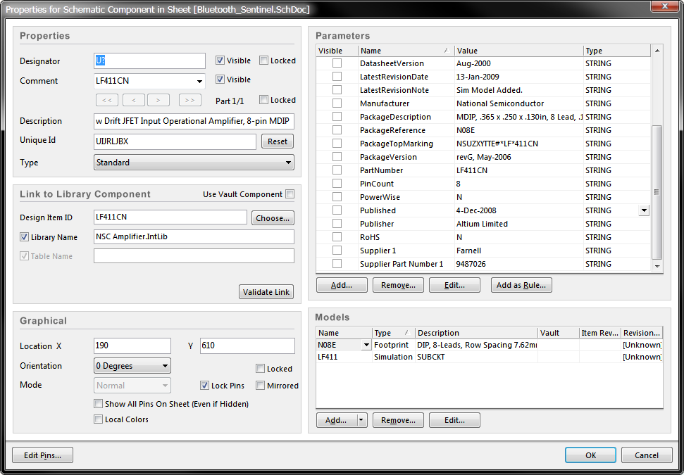
LF411in the Models list down the bottom right of the dialog, then click the Edit button below to display the SIM Model - General / Generic Editor dialog.
- Note that in the Model Location area of the dialog the Found In information shows that the model has been found in the integrated library. Click on the Model File tab at the bottom of the dialog to display the contents of the model file (shown below). If no model file has been found, an error message will appear in this tab. Altium Designer's simulator supports Spice 3F5 models, and most PSpice models.
- Click on the Netlist Template tab to show the netlist template. Each numerical value shown here is the number from the Model Pin list on the Port Map tab of the dialog.
- Click on the Netlist Preview tab, it shows how the detail will be written into the SPICE netlist, prior to simulating. Because the circuit is incomplete and has not been compiled, this detail will not be complete yet. What is shown in the schematic pin number from the component symbol, these are replaced by the name of the net connected to that pin once the circuit has been compiled.
- Click OK until all dialogs are closed. You are now ready to place the op amp on the schematic sheet.
- Position the op amp at a suitable location on the schematic sheet, and click to place. Tips on orienting a floating component are detailed below.
- Exit part placement mode by right-clicking or pressing the Esc key.
Adding a New SIM Model File
In almost every circuit design it is likely that you will need to use a simulation model file that has been sourced from outside the Altium libraries, for example from the device manufacturer's website. As well as model files stored within integrated libraries, discrete model files can be used. Note that you must use the correct file extension for each model type. For example, a SPICE .subckt will not be found unless it is in a *.ckt file, nor will a SPICE .model if it is not in a *.mdl file. It is recommended that you copy any model files received from a manufacturer into your design's project folder, which is automatically scanned for models when the circuit is simulated.
- For the sake of demonstration, we will add in another SPICE model, LF411C.ckt. At the end of this page is the source model data for an LF411C. Using a text editor, copy the content and paste into a text file, saving it with the name
LF411C.ckt. Save the file into the same folder as the other project documents. - Add the model file to the project by selecting the project name (
Filter.PrjPCB) in the Projects panel, right-click and select Add Existing to Project. In the Choose Documents dialog, set the filetype filter to All files (*.*). Select the model file and click Open. The SPICE model fileLF411C.cktis added to the project under the\Libraries\AdvancedSim Sub-Circuitsfolder in the Projects panel. Note that this is not required if the model is in the Projects folder, but must be done if the models are stored elsewhere, such as a central model storage folder.
We can now add the model to the component in the schematic. This could also be done in the Schematic library for this component, if required.
- Double-click on the op amp (U1) to open its Properties dialog. Delete the existing SIM model in the Models section by selecting it and clicking on Remove, and then confirm the deletion.
- Click the down arrow on the Add button in the Models List section to display a list of model-types, and select Simulation from the list.
- The SIM Model - General / Generic Editor dialog displays, as shown below.
- Select Spice Subcircuit from the Model Sub-Kind list to set the Spice Prefix to X and enable the Model Location fields. Note that the dialog name changes to reflect the Model Sub-Kind.
- Type
LF411Cin the Model Name field (no extension required) and select the Model Location of Any to search all available libraries and the current project directory for a matching model. Note that the file name is not used to search for the model, rather all.CKTfiles found in the valid locations are searched, for the.subckt LF411Cmodel declaration. - Altium Designer stops searching for a model as soon as a match is found. For all models not tied to an integrated library, the search will proceed to model files added to the project and then to model files found on the Search Paths as set up in the Search Paths tab of the Options for Project dialog (Project » Project Options). In this example, the search will find the model file LF411C.ckt located in the project folder, which will be detailed in the Found In field of the dialog.
Whenever a model search does not find a match, an error will appear in the Model File tab. An interactive error will also appear in the Messages panel when you compile the project.
- The final step is to check the pin mapping of the new model to make sure that it matches the pin numbering of the schematic component. Click on the Port Map tab of the SIM Model - General / Spice Subcircuit dialog to do this.
- Compare the detail shown in the Model File tab of the dialog, to the Schematic Pin and Model Pin details listed in the upper part of the dialog. Note that the numerical values used to identify the connections in the model file are not pin numbers, they are simply a unique numerical identifier for each connection in the model file. It is the order of the connections that is important, each Connection's position in the order is reflected by the numerical value shown in the Model Pin list. To map the pins,
- look at the function of each Schematic Pin,
- using the descriptive information in the comments section of the Model File tab at the bottom of the dialog, find that Connection,
- find its numerical position in the
.SUBCKTstatement (eg, 3 for the third connection), - then set the Model Pin numerical value in the upper part of the dialog to match (double click to edit).
- If the schematic symbol was a multi-part component, you would then repeat the process for each part in the package.
- When you have finished mapping the pins, click OK until all dialogs are closed.
We will now continue with creating the simulation-ready Filter schematic.
Adding the Simulation-ready Resistors
Next, we will place the two resistors.
- In the Libraries panel, make the
Miscellaneous Devices.IntLiblibrary the active library. - Set the component Filter by typing
resin the filter field just below the Library name. - Click on
Res1in the components list to select it, then click the Place Res1 button. You will now have a resistor symbol floating on the cursor. - Before placing, press the Tab key to open the properties dialog and edit the resistor's settings. In the Properties section of the dialog, set the Designator to
R1. - The circuit simulator does not use the component's Comment field to establish a discrete component's value, it looks for a Parameter called Value. Confirm that the resistor has a Parameter called Value, and set the value of this parameter to
100K. If there is no Value parameter, add one and set its value to100K. - Confirm that the Visible checkbox for the Value parameter is cleared (not enabled).
- To display this Value on the schematic instead of the Comment string, use the Comment field dropdown and select =Value from the list. This instructs Altium Designer to display the contents of the Value parameter in place of the Comment string. This will also be passed to the PCB to be used as the PCB component's Comment string.
- Confirm that the Visible checkbox for the Comment field is enabled.
- Now to check the SIM model in the Models list, down the lower right of the dialog. Locate the Simulation model and double-click to display the Sim Model - General/Resistor dialog. This type of resistor does not require a model file, and it takes the value required by the Netlist Template from the Value parameter.
- Click OK to close the Sim Model dialog and return to the component's Properties dialog. Click OK to close this dialog, ready to complete the placement of the resistor.
- Using the schematic image shown earlier on this page as a guide, position the resistor and left-click (or press Enter) to place the part. If required, press the Spacebar to rotate the component before placing it.
- Another resistor will appear floating on the cursor. Because you defined the designator of R1 during placement, the designator will automatically increment when you click to place R2, position and place it in a suitable location.
- Once you have placed the two resistors, right-click or press Esc to exit part placement mode.
Setting Up Simulation-ready Capacitors
Now to find and place the two capacitors.
- There is a suitable capacitor in the
Miscellaneous Devices.IntLiblibrary, which should already be selected as the active library in the Libraries panel. Type cap in the filter field in the Libraries panel. - Double-click on
Capin the components list to commence the placement process. - Before placing, press the Tab key to edit the capacitor's properties. In the Properties section of the dialog, set the Designator to
C1. - Edit the Value parameter to have a value 112pF, and clear the Visible checkbox.
- In the Properties section of the dialog, click on the Comment field and select the =Value string from the drop down list. Enable the Visible checkbox for the Comment field.
- Position and place the capacitor in a suitable location.
- A second capacitor will appear floating on the cursor, press Tab and change the value for C2 to
56pFfor C2. - If required, press the Spacebar to rotate the component before placing it, then place it in a suitable location.
- Right-click or press Esc to exit placement mode.
Adding the Voltage Sources
Now we can add the voltage sources needed to power the design when simulating.
- We will place the VDD power source first. To be able to do this, the simulation sources library must be made available. To make the library available, click the Libraries button at the top of the Libraries panel, opening the Available Libraries dialog.
- Click the Install button, then browse to the
\Library\Simulationfolder. This folder has a number of special simulation libraries, including; sources, math functions, PSpice functions and transmission lines. Locate and select theSimulation Sources.IntLibto add it to the list of Available Libraries, then click the Close button in the Available Libraries dialog. - In the Libraries panel, select the Simulation Sources.IntLib so that it is the active library, then browse through the contents, stopping on the VSRC component.
- Double-click on the VSRC to place it, pressing Tab to edit its properties before placement.
- Double-click on the SIM model VSRC in the Models list down the bottom right of the component's Properties dialog, the Sim Model - Voltage Source/DC Source dialog will open.
- Check that the Model Kind is set to Voltage Source and the Model Sub-Kind to DC Source.
- Click on the Parameters tab in the dialog to set up the required voltage value. Type
5Vin the Value field and enable its Component Parameter option. This instructs Altium Designer to automatically create the parameter Value for you in the Component Properties dialog. Enter 0 (zero) in the other fields.
- Click OK to close the Sim Model dialog.
- In the Component Properties dialog, enter the designator VDD, set the Comment to =Value, enable the Comment's Visible checkbox and click OK to close the dialog.
- Click to place this voltage source on the schematic, it will appear as shown below. For information about a source, or any other component placed from one of the special simulation libraries, press F1 when the cursor is over the component.
- The next task is to place the VSS power source. Use the same sequence of steps to place another VSRC, except this time the model Value parameter is
-5V, and the designator isVSS. - The last component to place is the Sinusoidal excitation Voltage Source. This is a VSIN component, which is also available from the
Simulation Sources.IntLib. Press Tab to edit its properties before while it is floating on the cursor, then double-click on the Simulation model to open the Sim Model - Voltage Source / Sinusoidal dialog and switch to the Parameters tab.
- Set the Frequency model parameter to
50KHzand the Amplitude to5, as shown in the image above. - Click OK until the dialogs are closed and click to place this voltage source on the schematic, as shown in the circuit at the top of this page.
- Right-click or press Esc to exit placement mode.
- Save your schematic [shortcut: CTRL+S].
Wiring Up the Circuit
Wiring is the process of creating connectivity between the various components of your circuit. For details of the wiring, refer to the circuit shown at the top of this page.
- Select Place » Wire [shortcut: P, W], or click on the Wire tool on the Wiring Tools toolbar to enter wire placement mode, as shown in the image below.
- When complete, right-click or press Esc to exit wire placement mode.
Adding Power Ports
Add the power ports as shown in the circuit image at the top of this page.
- Select Place » Power Port [shortcut: P, O], or click the VCC Power Port button on the Wiring Toolbar, as shown in the image below.
- While the Power Port is floating on the cursor, press Tab to open the Power Port dialog then edit the Net name, setting it to
VDD. Note that the Style can also be set to a variety of options, as shown in the image below. The Bar style will be used initially. Click OK to close the dialog.
- If required, rotate the floating Power Port by pressing the Spacebar.
- Place a VDD Power Port on pin 7 of U1, and a second one on the upper pin of the source VDD.
- Press Tab to open the Power Port dialog again, this time setting the Net name to VSS.
- Place a VSS Power Port on; the top of the VSS source, another on pin 4 of U1, and another on the lower pin of C2, as shown in the image at the top of the page.
- Press Tab to open the Power Port dialog again, set the Style to Power Ground and the Net name to
GND. - Place 3 GND Power Ports, one on each of the lower pins of the source components, as shown in the image at the top of the page.
- Press Tab to open the Power Port dialog again, set the Style to Circle and the Net name to
OUT. - Place the OUT Power Port on the output pin of the op amp, as shown in the image at the top of the page.
- When you have finished placing the power ports right-click or press Esc to exit placement mode, then save the schematic.
Adding Net Labels
Our last task before running a simulation is to place net labels at appropriate points on the circuit so we can easily identify the signals we wish to view. In the tutorial circuit, the points of interest are the IN and OUT nets. The IN net is identified with a net label while the OUT net name is read from the OUT power port.
To place net labels on the required nets as shown in circuit at the top of the page:
- Select Place » Net Label [shortcut: P, N], press Tab and enter the Net label name
IN. Click to place the net label on the wire between VIN and R1. Note that the bottom left corner of the Net Label selection rectangle is the electrical hot spot, this point must touch the wire. - Place Net Labels
AandBon the circuit, as shown in the circuit at the top of the page. These can be used to examine the function of the circuit at these points. - Right-click or press Esc to exit Net Label placement mode.
- Save your circuit. Save the project as well by right-clicking on the project name in the Projects panel, and selecting Save Project.
For more information about placing net labels, refer to the Tutorial - Getting Started with PCB Design.
Compiling the Project
Compiling a project checks for drafting and electrical rules errors in the design documents. We will use the default settings in the Error Reporting and Connection Matrix tabs of the Options for Project dialog (Project » Project Options).
- To compile the Filter project, select Project » Compile PCB Project.
- When the project is compiled, any warnings and errors generated will display in the Messages panel. If there are errors, check your circuit and ensure all wiring and connections are correct. Note that using the default settings will result in there being a No Driving Source Warning, as the op amp's non-inverting input pin only has passive pins connected to it. Double-click on the warning in the Messages panel to open the Compile Errors panel, where you can click on each pin in turn. As the designer you have to make a descision about how to resolve the warning, your choices include:
- Place a Specific No ERC directive on the net, instructing the compiler to ignore Nets with No Driving Source warnings/errors, only at this location. Note that there are a number of styles of Specific No ERC directives, allowing you to choose one that best suits the circumstance of the exception.
- Re-configure the Report Mode of the Nets with No Driving Source compiler violation check in the Options for Project dialog, setting it to No Report.
- Edit the resistor R1, then edit the pins and re-configure the pin that connects to the op-amp to be an Output pin. Note that doing this will result in an Output symbol being added to the resistor pin, which could confuse other designers who are working with the schematic.
- Keep a mental note of the warning and move on, as you know that it is not a problem.
- Save the schematic and the project.
Setting Up the Analyses
Altium Designer allows you to run an array of circuit simulations directly from the schematic. In the following sections of the tutorial, we will simulate the output waveforms produced by our Filter circuit.
- The simulation can be set up and run using the Design » Simulate » Mixed Sim menu command, or by clicking on the appropriate button on the Mixed Sim toolbar. If the toolbar is not visible, select View » Toolbars » Mixed Sim to display it.
The Mixed Simulator is configured and run from the Mixed Sim toolbar.
- With
Filter.SchDocopen in the Schematic Editor and the Mixed Sim toolbar displayed, click on the Setup button on the toolbar to display the General Setup page of the Analyses Setup dialog, as shown below. Note that the design is compiled first to generate the SPICE-format netlist (.NSX) before the dialog opens, the Messages panel will display any warnings or errors detected in the schematic. If required, close the Analyses Setup dialog, fix any issues, and then select the Setup tool again.
As well as general simulation options, the Analyses Setup dialog is used to enable and configure each simulation type.
All of the simulation options are set up in the Analyses Setup dialog, as well as the types of simulation analyses to be performed. General Setup simulation options include: what data is to be collected during the analysis process; the scope of the simulation (sheets to netlist); and the signals to be automatically displayed when the simulation is complete (active signals). These options are stored in the project file (when saved) and are used in the creation of the SPICE netlist (*.nsx) that is automatically generated when the simulation is run.
- First, we will set up the nodes in the circuit that we want to observe. In the Collect Data For dropdown, select Node Voltage, Supply Current, Device Current and Power from the list. This option defines what type of data you want calculated during the simulation run, i.e. it saves data for the voltage at each node, the current in each supply and the current and power in each device.
- Set the Sheets to Netlist option to Active project.
- Set the SimView Setup option to Show active signals.
- In the Available Signals field, double-click on the IN and OUT signal names. As you double-click on each one, it will move to the Active Signals field. You can also select multiple signals from the Available Signals list by clicking and dragging the mouse over the signal list, or using the SHIFT and CTRL keys while clicking on signals. Then use the > button to move the signals to the Active Signals list. The simulation results for Active Signals automatically display in the Waveform Analysis window when the simulation is run.
- In the Analyses/Options list, enable the Operating Point Analysis, Transient Analysis and AC Small Signal Analysis, as shown in the image below.
- Each individual analysis type listed in the Analyses/Options section is configured on a separate page of the Analyses Setup dialog. Click on the analysis name to activate the corresponding setup page.
Setting Up a Transient/Fourier Analysis
A Transient/Fourier analysis generates output like that normally shown on an oscilloscope, computing the transient output variables (voltage, current or power) as a function of time over the user-specified time interval.
An Operating Point analysis is automatically performed prior to a Transient analysis to determine the DC bias of the circuit, unless the Use Initial Conditions option is enabled. If this option is enabled, the DC bias is calculated from the initial conditions defined in the schematic. The initial condition can be defined for each appropriate component in the schematic, or .IC devices can be placed in the circuit.
To view six cycles of the 50KHz excitation voltage, we will set up to view a 60u portion of the waveform.
- Confirm that the Transient/Fourier Analysis is enabled (ticked). Click on the Transient/Fourier Analysis name in the Analyses/Options list to display the Transient/Fourier Analysis Setup page.
- Check that the Use Transient Defaults option is disabled, so that the Transient Analysis parameters can be modified.
- To specify a 60u second simulation window, set the Transient Stop Time field to
60u. - Set the Transient Step Time to
100n, indicating that the simulation calculates a point every 100ns. During simulation, the actual timestep is varied automatically to achieve convergence and the required accuracy. - The Maximum Step field limits the variation of the timestep size, set the Transient Max Step Time to
200ns.
Setting Up an AC Small Signal Analysis
An AC analysis generates output that shows the frequency response of the circuit, calculating the small-signal AC output variables as a function of frequency. The desired output of an AC small-signal analysis is usually a transfer function, e.g. voltage gain.
The schematic must contain at least one AC source with a value entered for the AC Magnitude parameter in its SIM model. We have already set up the parameters of our sinusoidal excitation source (VSIN) to contain the AC Magnitude value, frequency and amplitude, in the Adding the Voltage Sources section of this page.
- Confirm that the AC Small Signal Analysis option is enabled.
- Enter the Parameter Values as shown above.
When this analysis is run, an Operating Point analysis is run first to determine the DC bias of the circuit. The signal source is then replaced with a fixed amplitude sine wave generator and the circuit is analyzed over the specified frequency range, stepping in increments defined by the values in the Test Points and the Sweep Type fields.
Running the Simulation
You are now ready to run the enabled analyses.
- To run the simulation, click the Run Mixed Signal Simulation button on the Mixed Sim toolbar. Note that if you opened the Analyses Setup dialog by selecting the Design » Simulate » Mixed Sim menu command, then the simulation is performed when you click to Close the dialog. Otherwise, use the Run button on the toolbar.
Any warnings or errors produced during the generation of the SPICE netlist, or the actual simulation process itself, will be displayed in the Messages panel. Fix any errors before proceeding.
- If there are no errors in the circuit, a SPICE netlist (
*.nsx) is created and passed to Altium Designer's simulation engine. Note that the netlist is regenerated each time a simulation is run. The simulation begins and a simulation data file (*.sdf) will open. The results of each analysis are shown as a separate chart in the SimData Editor's Waveform Analysis window. The Operating Point analysis is performed first to determine the DC bias of the circuit. - When the simulation is finished, you should see outputs similar to those shown below.
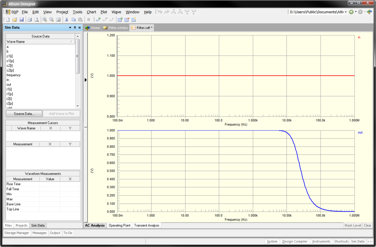
Simulation results are displayed in the Waveform Analysis window (SDF), with each enabled analysis type displayed on a separate tab - the AC Analysis is shown above.
The Operating Point analysis is simply a list of Active Signals and their values.
![]()
The Transient Analysis waveforms.
Summary of Working with Waveforms
The right-click menu includes commands are used to configure each aspect of the Waveform Analysis window, the arrows show what aspect each command will modify.
It is very easy to reconfigure the waveforms in the Waveform Analysis window. The right-click menu is context sensitive (shown above), for example the Plot Options command will apply to the Plot under the right-click location. Similarly, there are different right-click commands presented when you right-click on an Axis.
A waveform can be moved from one plot to another using click and drag.
- For example, to display the IN and OUT waveforms on the same Plot, click and hold on the OUT waveform in the lower plot of the AC Analysis chart, and drag and drop it onto the upper plot, as shown below.
Click and drag to move a waveform from one plot to another. Note that the plots are displayed in bold to make them more visible on this web page (Tools » Document Options).
Creating a Bode Plot
The default display mode for the AC Analysis chart has the voltage as a linear magnitude. This can be changed, for example to display the magnitude in decibels, as used in a Bode Plot. A Bode plot consists of two curves — the log of magnitude (gain) and phase — as functions of the log of frequency. The gain in decibels (dB) and the phase are plotted along the Y axis on a chart that has several cycles of a log scale on the X axis. Each cycle represents a factor of ten in frequency.
The first step is to change the magnitude of the IN and OUT waveforms to decibels.
- Double-click on the IN waveform label shown on the right of the plot to open the Edit Waveform dialog.
- Select Magnitude (dB) from the Complex Functions list. Click the Create button to close the dialog and display the waveform in dB(net_name), i.e. dB(in), on the plot.
- Repeat this process for the OUT waveform.
- The empty lower plot will be used to display the phase. Add the IN wave to the empty plot by right-clicking on the plot and selecting Add Wave to Plot.
- The Add Wave to Plot dialog will open, select
infrom the list of Waveforms, select Phase (Deg) in the Complex Functions list, and click Create. - Repeat this process to add OUT to the lower Plot, as shown below.
- These waveforms can also be displayed on different Y axes, if required. This is done when the wave is being added to the Plot, by enabling the Add to new Y axis option in the Add Wave to Plot dialog. To remove the new Y axis, right-click on the axis and select Delete Axis. All waves that are plotted to this axis are removed, as well as any measurement cursors attached to these waves.
Multiple Y Axes can be defined, if required.
Using the Measurement Cursors
Now we can determine the 3dB point using the measurement cursors.
- Right-click on the dB(out) wave and select Cursor A. Position cursor A in the lowpass section by dragging the marker, as shown above (the location is not critical, as long as it is in the lowpass region).
- Right-click on the dB(out) wave again and select Cursor B.
- The Sim Data panel will be used to help locate the cursor, if it is not visible select View » Workspace Panels » Editor » Sim Data from the menus to display it.
- While watching the B-A Measurement value in the Sim Data panel, click and drag Cursor B to give a Y (gain) value of -3.
- Looking at the Measurement Cursors region of the panel, it can be seen that the X result for Wave Name B is 20.178k, indicating that the 3dB point of the filter circuit is 20kHz.
Use the cursors to read information from the waveforms.
- To clear the cursors, right-click on each cursor marker and select Cursor Off.
Running a Parameter Sweep Analysis
Another valuable design use of the circuit simulator is to perform parameter sweep. This allows you to explore variations in component values without editing the circuit multiple times. In a Parameter Sweep analysis the value of a device is changed in defined increments, over a specified range. AC, DC, or Transient analyses must also be enabled in order to perform a Parameter Sweep analysis, as the simulator performs multiple passes of each enabled analyses.
- Click on the Filter.SchDoc tab to make the schematic the active document in Altium Designer.
- Click on the Setup Mixed-Signal Simulation button to open the Analyses Setup dialog.
- Click on Parameter Sweep in the Analyses/Options section of the dialog to enable this analysis type and display the settings.
- Enter the parameter to be swept in the Primary Sweep Variable field. In this example, we will primary sweep parameter
C2[capacitance], double-click on the Value field to show the drop-down, and select it from the list. - To define the range of values for the sweep, set the Primary Start Value to
20pand Primary Stop Value to-20p. Set the Primary Step Value to define step increments to-10p. - Set the Primary Sweep Type option to
Relative Values. Doing this means that the values entered in the Primary Start Value, Primary Stop Value and Primary Step Value fields are relative to the parameter's existing or default value. - Click on Enable Secondary to add secondary sweep values. When a Secondary parameter is defined, the Primary parameter is swept for each value of the Secondary parameter.
- Set up the Secondary Sweep Variable for
C1[capacitance], to have a Secondary Start Value of -80p, Secondary Stop Value of80p, Secondary Step Value of80p, and the Secondary Sweep Type to beRelative Values.
- Click OK to close the dialog, then click the Run Mixed-Signal Simulation button on the Mixed SIM toolbar to run the simulation. Each primary sweep appears as a waveform with the notation <net_name_p<sweep_number>, e.g. out_p01, in a new plot in the AC Analysis and Transient Analysis tabs of the Waveform Analysis window.
- The Transient Analysis results will be displayed by default, switch to the AC Analysis results.
- Click on a sweep parameter name to display more information, for example clicking on
out_p10highlights that wave and displays the sweep information underneath the plot. Note that if you hover the mouse over a wave name, it will also display the sweep information in the tooltip, as shown below. You can also use the arrow keys on the keyboard to step through the series of waveforms.

Information about the swept component value(s) is displayed below the plot (if the wave is selected), or by hovering the cursor.
Using Advanced Options
The Advanced Options page in the Analyses Setup dialog contains a list of internal SPICE options that can be set to effect the simulation calculations, such as error tolerances and iteration limits.
- To change the value of a SPICE option, click one on the Value field to select it, it should then be ready for editing.
An example of when you might need to change the Advanced Options would be if you have a circuit design with unexpected high frequency oscillations, in this case you could change the standard Integration method from Trapezoidal to Gear. The Trapezoidal method is relatively fast and accurate, but tends to oscillate under certain conditions. The Gear methods require longer simulation times but tend to be more stable. Theoretically, the higher the Gear order, the more accurate the results but the simulation time increases.
Using a SPICE Netlist for Simulation
You can also perform a simulation directly from a SPICE netlist, allowing you to use the Altium Designer simulator in conjunction with other schematic capture tools. To do this:
- Include the netlist in an Altium Designer PCB project (.PrjPCB). To do this; create a new project, then right-click on the project name in the Projects panel and select Add Existing to Project and add the SPICE-format netlist (you will need to change the file type filter to see the .NSX file). Using a project allows you to save setup information between simulation sessions as the setup information is stored in the project file. If the netlist is opened as a free document, setup information is not stored between simulation sessions. Note that a project file is automatically added when you run simulation for the first time from P-CAD.
The Altium Designer simulation engine requires a netlist that includes the component information, design connectivity, and the model data, as well as the setup information. If there is no simulation setup information already contained in the netlist when you select Simulate » Run from the text editor menus, a new netlist is created named <original filename>_tmp.nsx. This file contains setup information from the Simulation Analyses dialog (stored in the project file), plus the netlist information from the original .nsx file.
If there is simulation setup type information present in the netlist, then the simulation is run directly from the source netlist. This is useful for advanced users who want to be able to modify settings directly in the netlist. Note that you can not add or configure setup information using the Analyses Setup dialog if the netlist already includes any setup information.
If there is no simulation setup information contained in the netlist but there are schematic documents in the project, then the netlist is regenerated from the schematic documents and the project's setup information. This would only occur if you deleted the setup information from the netlist and then attempted to simulate from it.
- Once you have added a netlist which has no setup information to a project, you can configure the analyses by selecting Simulate » Setup from the text editor menus.
- To run a simulation, select Simulate » Run from the menus. The simulation waveforms will display in a .sdf document.
- Rename the netlist file so it is not overwritten next time you run a simulation.
Example Model File
Below is the source model data for an LF411. Using a text editor, copy the content from this page and paste into a text file, saving it with the name LF411C.ckt.
*LF411C *Sngl LoOffset LoDrift JFET OpAmp pkg:DIP8 3,2,8,4,6. pkg:CAN8 3,2,8,4,6. * * Connections: * Non-Inverting Input * | Inverting Input * | | Positive Power Supply * | | | Negative Power Supply * | | | | Output * | | | | | .SUBCKT LF411C 1 2 3 4 5 C1 11 12 3.498E-12 C2 6 7 15E-12 DC 5 53 DX DE 54 5 DX DLP 90 91 DX DLN 92 90 DX DP 4 3 DX BGND 99 0 V=V(3)*.5 + V(4)*.5 BB 7 99 I=I(VB)*28.29E6 - I(VC)*30E6 + I(VE)*30E6 + + I(VLP)*30E6 - I(VLN)*30E6 GA 6 0 11 12 282.8E-6 GCM 0 6 10 99 1.59E-9 ISS 3 10 DC 195E-6 HLIM 90 0 VLIM 1K J1 11 2 10 JX J2 12 1 10 JX R2 6 9 100E3 RD1 4 11 3.536E3 RD2 4 12 3.536E3 RO1 8 5 50 RO2 7 99 25 RP 3 4 15E3 RSS 10 99 1.026E6 VB 9 0 DC 0 VC 3 53 DC 2.2 VE 54 4 DC 2.2 VLIM 7 8 DC 0 VLP 91 0 DC 30 VLN 0 92 DC 30 .MODEL DX D(IS=800E-18) .MODEL JX PJF(IS=12.5E-12 BETA=250.1E-6 VTO=-1) .ENDS LF411C