Configuring and Working in 2D or 3D Layout Mode
Historically, PCBs have been laid out in a 2-dimensional workspace that uses colors to represent the various layers of the PCB. But the physical PCB is a 3 dimensional object, requiring the PCB designer to take the multiple-layer, 2D representation on the screen and map that to a 3D representation in their mind. This challenge was alleviated to some extent by the 3D visualization features offered by some ECAD vendors, including earlier versions of Protel/Altium, but these visualization tools did not support true, 3D design.
The substantial improvements in 3D video card and the supporting software technology has allowed Altium to develop a solution to this problem - true, 3 dimensional PCB editing. More than simple visualization, Altium Designer's 3D capabilities allow the designer to:
- Perform 3D clearance checking, components can be critically aligned with each other and the enclosure, as required.
- Visually locate connectors and other components requiring access for servicing.
- Manufacturing processes and the order of assembly can be better defined knowing all mechanical constraints have been accounted for.
- More detailed hand assembly instructions, user manuals and instructions can be generated using images that are much closer to the reality of what will be seen by a human.
- Experiments with different colored solder masks can be made in order to create a more aesthetically pleasing product that works well with its enclosure and surroundings.
- Stakeholders are more easily brought onside when presented with a more concrete view of the end product.
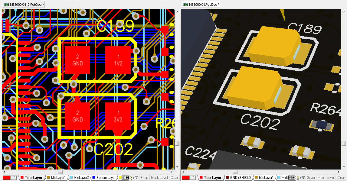
2D and 3D views of the same region of a board.
Altium Designer Display Modes
Related articles: PCB Layer Stack Management, Working with the Board Insight System
Altium Designer supports displaying and editing the board in 2D or in 3D, these are referred to as display modes. Display modes can be switched in the View menu, or using the shortcuts detailed below.
There are actually 3 display modes, each with a distinct function:
Board Planning Mode (press 1) - use this mode to define the board shape, and also to position and configure split lines and bending lines on a rigid-flex design. Split lines are used to divide the board into regions, each region can then be assigned a different layer stack. To learn more about board regions, and split lines and bending lines, refer to the PCB Layer Stack Management article.
2D Layout Mode (press 2) - the traditional 2D, multiple-layered view of the PCB. Altium Designer incorporates a set of features to help you manage your view of the board, called the Board Insight System.
3D Layout Mode (press 3) - the true, 3 dimensional design mode. Combine the 3D display mode with a 3D mouse, such as the Space Navigator from 3Dconnexion, to view and manipulate the loaded, 3 dimensional board, as if you were holding it in your hand.
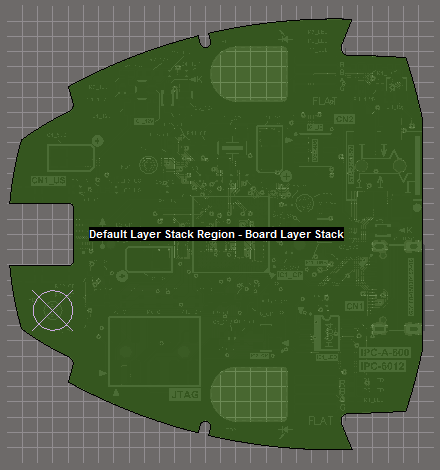
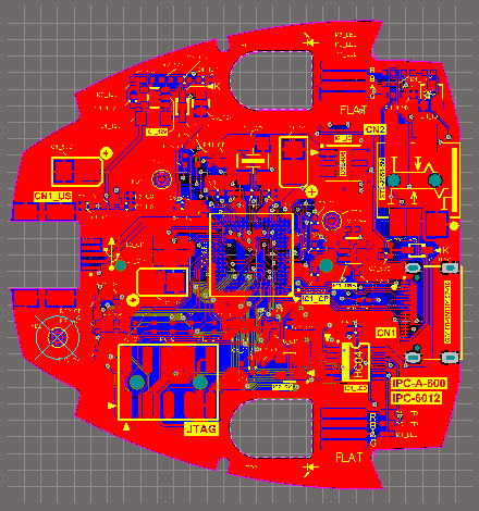
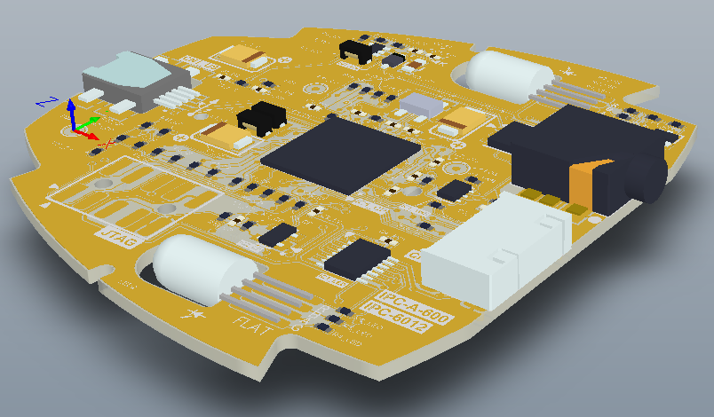
The same board shown in board planning mode, 2D mode, and 3D mode, each mode offers its own functions and advantages.
Single Layer 2D Display Mode
The traditional, 2-dimensional PCB design workspace uses colors to represent the various layers of the PCB. Because of the visual clutter that a multi-colored, 2D view can bring, Altium Designer offers a number of single layer modes too.

One approach to coping with the visual clutter is to switch to single layer mode. These images show the regular multi-layer display, then the 3 available single layer display modes, Gray Scale, Monochrome, and Hide Other Layers.
There are 3 different single layer modes available:
- Hide Other Layers - all other layers are hidden, only the contents of the active (current) layer are shown.
- Gray Scale Other Layers - all other layers are displayed in a shade of gray derived from their current layer color, the active layer is shown in its standard color.
- Monochrome Other Layers - all other layers are displayed in the same shade of gray, the active layer is shown in its standard color.
Single layer modes are enabled in the PCB Editor — Board Insight Display page of the Preferences dialog. This is an environment setting, it applies to all designs edited in this installation of Altium Designer.

Enable which Single Layer Modes are available in the Preferences dialog.
The currently chosen Single Layer Mode can be seen, and you can also switch modes, in the View Options tab of the View Configuration dialog. The settings in this dialog are stored in the PCB design file, so your selected mode will be retained then next time you open the board.
Examine the current Single Layer Mode, and switch modes in the View Configurations dialog.
Single Layer 3D Display Mode
Main article: 3D Single Layer Mode
Single layer mode is also available when the board is displayed in 3D Layout Mode. Use this for tasks such as examining the quality of routing on a specific layer, or the quality of a power plane layer. While in single layer mode, use the Ctrl+Shift+Wheel Roll shortcuts to step through the layers.
Single layer mode can also be used when the board is displayed in 3D.
Techniques for Displaying and Identifying Design Data
Main article: Board Insight System
To the casual observer, a PCB design is quite unintelligable - appearing as a mass of lines, circles, arcs and strings, appearing in different colors, all jumbled on top of one another. Even with a highly trained eye, it can be difficult to make sense of the vast amount of design detail. Altium Designer includes a number of features to help find, identify, and manage the display of design content, collectively these features are known as the Board Insight System.
2D Board Insight features includes:
- Insight Lens - use the Lens to examine an area of the board in detail, zoom in and out, switch to single layer mode and step through the layers (Shift+M to toggle).
- Insight Panel - displays detailed information about the components, nets and violations under the cursor (PCB Panels » Board Insight).
- Insight Pop-up - also displays displays detailed information about the components and nets (Shift+X), and violations (Shift+V) currently under the cursor, in a pop-up window instead of a panel.
- Heads Up Display - presents (configurable) detail about the objects currently under the cursor (SHift+H to toggle, PCB Editor - Board Insight Modes).
- Single Layer mode -displays just the current layer, other layers can be hidden, grayscaled or monochromed (PCB Editor - Board Insight Display).
- Live Highlighting - highlight all objects in the net under the cursor, including their locked status (PCB Editor - Board Insight Display).
- Enhanced object labeling - display detail on objects in the workspace, including: net name, pad number, testpoint status, component origin (View Configurations, View Options tab).
- Layer Transparency - allows you to see though objects to other objects underneath (View Configurations, Transparency tab).
3D Board Insight features include:
- 3D Visualization panel - displays 3 simultaneous views of the board in 3D, 2 of which are cross-sections (PCB Panels » 3D Visualization).
- Project modes - display the board using Perspective or Orthographic projection (View Configurations, Physical Materials tab).