PCB Design View
Contents
- Placing a Design View
- Defining the View Area
- Setting the Location and Scale of the Design View
- Defining the Title
- Interactively adjusting the Scale, Size and Focus of the Design View
- Placing a View of the Bottom Side of the Board
- Placing a Design View of a Different PCB Document
- Including a Design View in Printed or PDF Output
- Displaying/Hiding a Design View
A modern PCB can be compact, dense and small in size, making it difficult to present important design information in the documentation. To help in this process the PCB Editor supports placing a specific view of a PCB design within the workspace, which can then be included in documentation output. This view is called a Design View, allowing the designer to place a snapshot of any rectangular shaped region of the current board, or another board. The Design View can be placed anywhere in the workspace and scaled to any size.
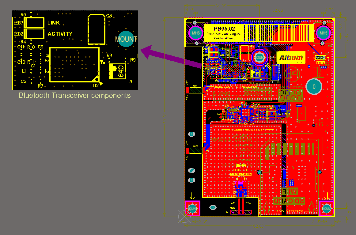
Place a Design View to show a specific area of the board, this one is double the size.
Placing a Design View
Select Place » Design View from the PCB Editor menus to place a Design View in the current PCB workspace. The Design View dialog will open, as shown below.

Configure the Design view manually or click the Define area button to specify the area, then click OK to place the View in the workspace.
Configure the settings (as described below) and click OK to place the Design View. Once the View has been placed you will return to the Design View dialog, ready to place another. Click Cancel to stop placing more Design Views.
Defining the View Area
The Design View dialog supports 2 modes of area definition, either by:
- Manually entering in the Width, Height and lower-left X and Y coordinates in the fields located in the image area of the dialog,
- Clicking the Define area button, which returns you to the workspace with a crosshair cursor, and then defining the rectangular region of the view.
Once the area has been defined, click OK to place the Design View in the workspace.
Setting the Location and Scale of the Design View
The initial location of the Design View is defined interactively when it is placed. The Location settings in the dialog can be used to accurately position the Design View once it has been placed.
The Scale can defined in the dialog, or interactively configured once the View has been placed in the workspace.
Defining the Title
The Design View can have its own Title, in a user-defined Font, Color and Height. Configure these as required in the Design View dialog.
Interactively adjusting the Scale, Size and Focus of the Design View
Once a Design View has been placed in the workspace, you can interactively adjust the scale, size and focus of the View.
- Adjusting the Scale - click once to select the Design View, then Click and Drag on a corner handle to scale the Design View up (drag out) or down (drag in).
- Adjusting the View Size - click once to select the Design View, then Ctrl+Click and Drag on a corner handle to resize the Design View without changing the scale.
- Changing the Focus - Ctrl+Click and Drag anywhere within the Design View to slide the currently viewed area around within the Design View window.
Ctrl+Click and Drag to slide and adjust the area currently being viewed in the Design View.
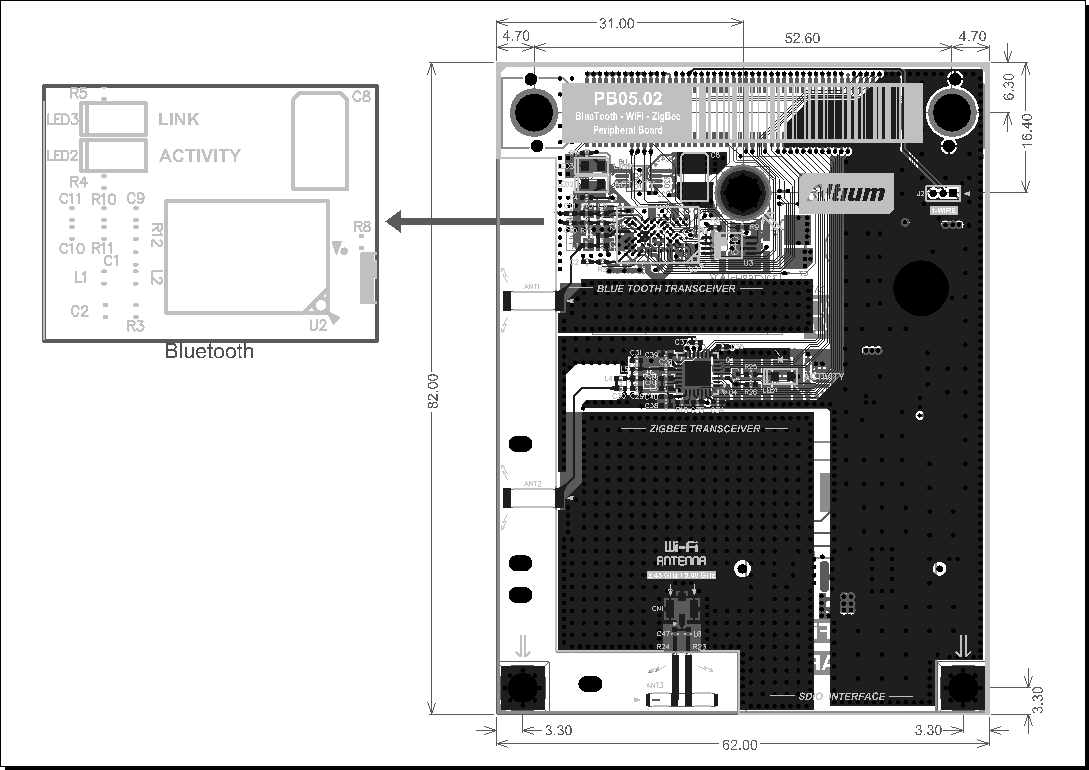
Placing a View of the Bottom Side of the Board
Design Views support mirroring, that is showing a flipped image of the board. Use this feature when you need to show a view of the bottom side of the board. On approach to this is to have the board displayed looking from the top, then:
- Select Place » Design View, the Design View dialog will open,
- Cclick the Define Area button, interactively define the rectangular region to be displayed,
- The Design View dialog will re-appear, enable the Mirror checkbox
- Select the Layers tab and enable the required layers
- Click OK to close the dialog,
- Place the Design View in the workspace.
Use a Design View to display an area on the bottom side of the board.
Placing a Design View of a Different PCB Document
The default behavior when placing a Design View is to place a view of the current PCB. To place a View of a different PCB:
- Select the Specify Document option,
- Then click the button to open the Choose PCB Design File dialog,
- Locate and select the target .PcbDoc file,
- Click the Open button to complete the selection, and return to the Design View dialog,
- Configure the Width, Height and lower-left X and Y coordinates in the fields located in the image area of the Design View dialog,
- Click OK in the Design View dialog to place the view of the other board in the current workspace.
Including a Design View in Printed or PDF Output
Design Views are included in printed and PDF output. The Design View retains its own layer visibility settings in the output, allowing it to present as the designer requires in the printed/PDF output. Note that the primitives on layers used in the Design View continue to obey the display settings defined in the Layer Properties dialog for that layer in the PCB Printout Properties settings defined for that output. For example, if the Top Overlay is displayed in the Design View, and the Top Overlay is configured to display tracks in Draft mode for that output in the Output Job, then the Top Overlay tracks in the Design View will also present in Draft mode.
Design Views are included in printed or PDF type output.
Displaying/Hiding a Design View
Design Views that have been placed in the workspace can be hidden if required, toggle the Show Design Views option in the Show/Hide Tab of the View Configurations dialog. Note that a Design View that is hidden is still included in a printout or PDF.
Disable the Show Design Views option to hide all Design Views currently placed in the workspace.