PCB
Contents
- Summary
- Panel Access
- Panel browsing modes
- Setting the visual filtering
- Filter options
- Panel mini-viewer
- Browsing Nets
- Managing xSignals
- xSignal Classes region
- xSignals region
- xSignal Primitives region
- Create xSignals in Nets mode
- Browsing Components
- Using the From-To Editor
- Adding From-Tos
- Choosing a Predefined Topology
- Using the Split Plane Editor
- Using the Differential Pairs Editor
- Managing Differential Pairs
- Creating Differential Pairs from Design Nets
- Configuring Applicable Design Rules
- Browsing Polygons
- Using the Hole Size Editor
- Browsing 3D Models
- Browsing Layer Stack Regions
- Right-Click Menus
- Notes
Parent page: Panels

The PCB panel gives you full access to board objects, items and classes via a filtered browser.
Summary
The PCB panel allows you to browse the current PCB design using various filter modes to determine which object types or design elements are listed, highlighted or selected. It also has editing modes for certain object types or design elements that provide you with specific controls on the panel for editing procedures. Note, you can still access the properties for any element listed in this panel.
Panel Access
To display the PCB panel, click the PCB button ![]() at the bottom-right of Altium Designer when the PCB Editor is active, and select the PCB entry from the pop-up menu. Alternatively, you can access the panel through the View » Workspace Panels » PCB » PCB sub-menu.
at the bottom-right of Altium Designer when the PCB Editor is active, and select the PCB entry from the pop-up menu. Alternatively, you can access the panel through the View » Workspace Panels » PCB » PCB sub-menu.
Use the PCB button then the PCB menu option to open the PCB panel
Panels can be configured to be floating in the editor space or docked to sides of the screen. If the PCB panel is currently in the group of docked Workspace panels on the left, use the PCB tab located at the bottom of the panels to bring it to the front.
If already open and docked in the Workspace panels, use the PCB tab to access the PCB panel.
Panel browsing modes
The top drop-down list in the panel is where you select the panel mode. The mode can be set to browse Nets, Components, Polygons, 3D models (3D bodies) or Layer Stack Regions, or set to use the From-To, Split-Plane, Differential Pairs, and Hole Size Editors.
Select the browsing mode using the top pull-down list.
In any of the modes, as you click on an entry in a subsequent region of the panel, a filter is applied, essentially using the entry as its scope.
Setting the visual filtering
The visual result of the applied filtering on the document in the design editor window is determined by a series of highlighting controls toward the top of the panel. The effect that is imposed in the editor can be set to Normal, Mask or Dim, where in practice, Mask has the most obvious highlighting effect.
The Normal / Mask / Dim dropdown list provides you with options for visibly contrasting filtered and unfiltered objects within the design editor window. To change the masking and dimming options see the Highlighting Options area in the PCB Editor - Display page of the Preferences dialog.
Select the type of visual filtering applied using the masking mode drop-down list.
The visual highlighting effect for each masking mode:
- Normal - When Normal viewing mode is selected, filtered objects are highlighted, however, the appearance of unfiltered objects remains unchanged.
- Mask - When Mask viewing mode is selected, filtered objects will appear visible in the design editor window, with all other objects being made monochrome
- Dim - When Dim viewing mode is selected, filtered objects will appear visible in the design editor window, with all other objects retaining their colors, but being shaded.
Controls for adjusting masking and dimming are accessed from the Mask Level button ![]() (bottom right of design editor window). Note, this option is not available when using the panel in From-To Editor mode.
(bottom right of design editor window). Note, this option is not available when using the panel in From-To Editor mode.
Control of the visual masking and dimming levels in the Mask Level control panel.
For each masking mode (Dim and Mask) the panel has two controls to set the contrast between filtered and unfiltered objects:
- When Mask viewing mode is selected, the Masked Objects Factor slide control determines the level of shade applied to unfiltered objects and the Background Objects Factor slide control determines the level of visibility of unfiltered objects. In this mode, unfiltered objects will be unavailable for selection or editing.
- When Dim viewing mode is selected, the Masked Objects Factor slide control determines the level of shade applied to unfiltered objects and the Highlight Objects Factor determines how white the filtered objects highlighting will be.
Filter options
The panel's three check boxes apply these filter options:
- Select - when enabled, the filtered objects will be selected in the workspace. This option is not available when using the panel in From-To Editor mode.
- Zoom - when enabled (default), the filtered objects will be zoomed and centered (where possible) in the design editor window. Use the Zoom Level button to adjust the zoom factor that will be used to close-in on filtered objects.
- Clear Existing - when enabled (default), any existing filter will be cleared before applying a new one. Disabling this option allows you to extend an existing filter, essentially refining the filter further by applying a new filter in addition to the existing one. This option is not available when using the panel in From-To Editor mode.
Any combination of these options can be enabled. For example, you might want to have all filtered objects zoomed, centered and selected in the design editor window, whilst applying masking to take away the clutter of other design objects.
Use the Clear button to clear the currently-applied filter. All objects in the design workspace will become fully visible and available for selection/editing. If you wish to re-apply the filter, click on the Apply button.
Panel mini-viewer
The bottom section of the PCB panel provides a mini-viewer for the current document, with an image of the PCB board central to its window. A white viewing box is imposed on the image to show the area currently displayed in the design editor window. As the editor display automatically pans and zooms in response to the PCB panel filter selections, the box moves and expands accordingly to indicate the board viewing area.
The mini-viewer automatically window pans and zooms to reflect the status of the main editor window.
As you manually pan around the document in the design editor window - using the editor's horizontal and vertical scroll bars or the right-click panning hand - the viewing box in the panel will also move accordingly. Conversely, if you click inside the viewing box and drag it around the board image, the document in the design editor window will be panned accordingly, and at the current zoom level.
As you zoom in or out in the design editor window, the viewing box will be resized accordingly in the panel. Conversely, resizing the viewing box in the panel, by clicking and dragging on any of its vertices, will cause the zoom level to change in the design editor window. The smaller the size of the viewing box, the more the actual document has been zoomed-in.
Browsing Nets
Select Nets from the PCB panel's drop-down list. The three main list regions of the panel will change to reflect an object hierarchy, in order from the top:
- Net Classes, as defined by the board.
- Individual member Nets within a class.
- Individual items within a Net (pads, vias, tracks and fills).
The PCB panel regions allow a cumulative filter selection through net classes, to individual nets, to net items (primitives).
Right-clicking on a net or net item entry and choosing the Properties command from the subsequent pop-up menu (or double-clicking on the entry directly) will provide access to the relevant properties dialog, from where you can view or modify the properties of the net/item as required.
Right-clicking on a net class entry and choosing Properties from the menu (or double-clicking on the entry directly) will open the Edit Net Class dialog for that class. From this dialog you can view/modify the net membership of the class, rename it, or add additional classes.
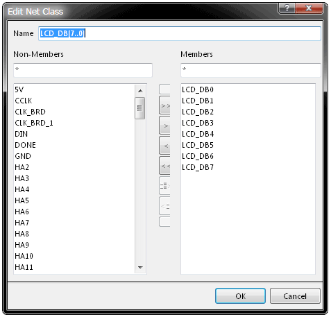
Editing a selected net class.
The display/inclusion of each net item type, in the Net Items region of the panel, is dependent on whether the corresponding option for each has been enabled on the right-click menu, accessed from either the Nets or Net Items regions.
Right-click on a net or net item entry to select the included items.
Note that the Primitive list right-click context menu also offers the option to create an xSignal between two selected items – see Create xSignals in Nets mode below.
In summary, as you click on an entry in the panel's list, a filter will be applied based on that entry. The visual result of the selection (in the design editor window) is determined by the highlighting methods enabled (Mask/Dim/Normal, Select, Zoom). Multiple entries can be selected in each region, using standard SHIFT + Click and CTRL + Click features.
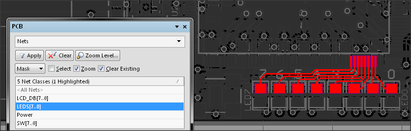
A net class LED[7..0] selected with the visual mode set to Mask.
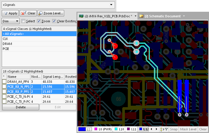
Managing xSignals
Place the panel in xSignals mode by selecting xSignals from the drop-down list at the top of the panel.
An xSignal is essentially a designer-defined signal path between 2 nodes - they can be 2 nodes within a net, or they can be 2 nodes in associated nets separated by a component. The defined xSignal can then be used to scope relevant design rules such as Length and Matched Length, which will then be obeyed during design tasks, such as interactive length tuning.
xSignals are used define a complete signal path, from source to destination, while incorporating branches or terminating/matching components that connect individual nets. The complete signal path can then be treated as a single high-speed connection between two points (typically from a source pad to destination pad).
See High Speed Design with xSignals for more information on the philosophy behind xSignals and how they are defined.
In the PCB panel’s xSignals mode, its three main list regions change to reflect the xSignal object hierarchy, in order from the top:
- xSignal Classes.
- Individual xSignal definition within a class.
- Individual primitives that constitute an xSignal (pads, tracks and vias).
In xSignal mode, the PCB panel regions allow a cumulative filter selection through xSignal classes, to individual xSignals, to constituent xSignal primitives.
xSignal Classes region
The xSignal Classes region lists any xSignal class collections that have been defined, or simply all available classes (<All xSignals>).
Select a class to see its xSignals list in the middle panel region (xSignals) and to display them in the PCB workspace.
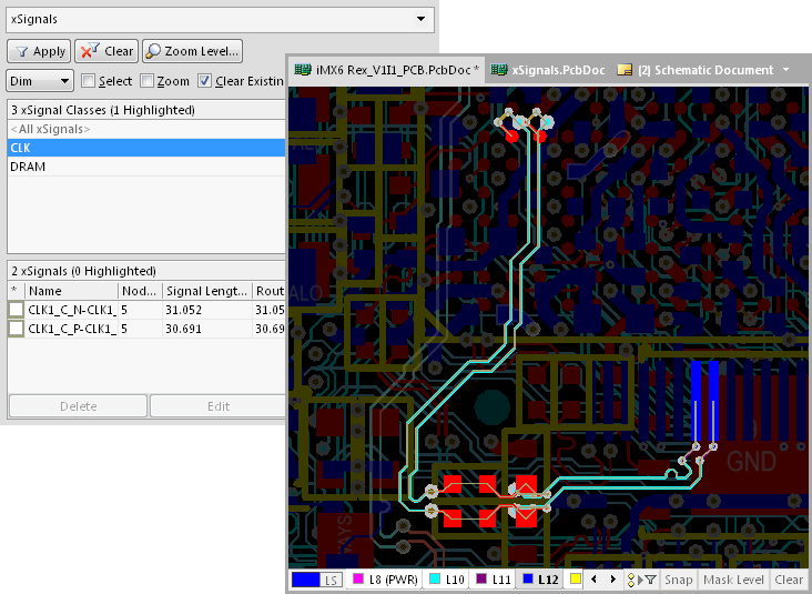
Selecting an xSignal class will list its members in the panel's xSignals region and highlight them in the PCB worlspace.
To create a new xSignal class from the existing xSignal collection, right-click in the region and select Add Class from the context menu. The Edit xSignal Class dialog lists the available xSignals which can be added as members to the new class using the ![]() and
and ![]() buttons – use the Name field to define a suitable name for the new xSignal class.
buttons – use the Name field to define a suitable name for the new xSignal class.
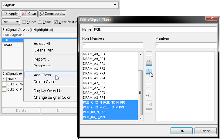
Create or add to an xSignal class by adding/removing xSignal members via the Edit xSignal Class dialog.
The panel region’s right-click context menu also offers the ability to remove (Delete) or rename (Properties) an xSignal class, and change its visual representation in the PCB workspace (for example; Change xSignal Color)
xSignals region
The panel’s xSignals region lists all defined xSignals for the design, and their individual details such as signal/routing lengths and number of nodes. Note that multiple xSignals can be selected using standard Shift and Ctrl –click techniques – the multiple selections are visually shown in the PCB workspace.
Defined xSignals can be selected and managed in the panel's xSignal region.
xSignal Primitives region
The PCB panel’s third region, xSignal Primitives, lists all the constituent elements (primitives) of the currently selected xSignal.
Select the region’s Show nodes only checkbox to restrict the primitives listing to pads that are the xSignal start/end point nodes. In this mode the selected xSignal will be shown in the PCB workspace as node pads joined by a thin trace (rather than tracks) that represents the xSignal path.
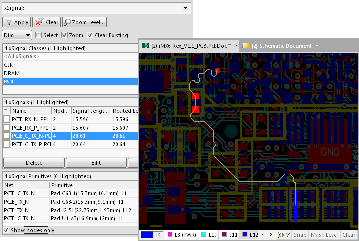
The lower xSignal Primitives region lists all elements of the selected xSignal, such as pads, vias and tracks.
Create xSignals in Nets mode
While xSignals are generally defined through the Create xSignals dialog (Design » xSignals » Create xSignals), they can also be defined manually using the PCB panel in Nets mode.
The below diagram shows two nets that form one half of a differential pair that couples a processor to a high-speed connector. As a high-speed connection, we want the two nets and series component defined as a one xSignal, so it can be used to scope design rules.
The two highlighted nets, PCIE_C_TX_N and PCIE_TC_N, are joined by series component C63. When selected in the PCB panel in Nets mode, the two nets are highlighted in the PCB workspace, as shown.
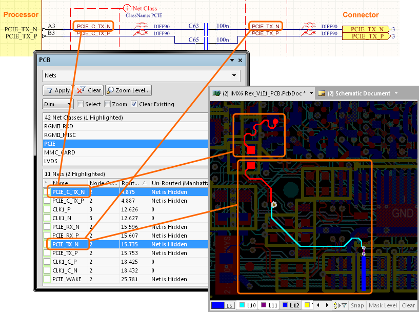
The complete path for one side of a differential pair is two nets joined by a series component.
To create a suitable xSignal, select the source and destination pads in the panel’s Primitives region, right-click on the selection and choose Create xSignal from the context menu. Note that the source is a pad on U1 (the processor) and the destination pad is on connector J2, and also that the two pads are in different nets.
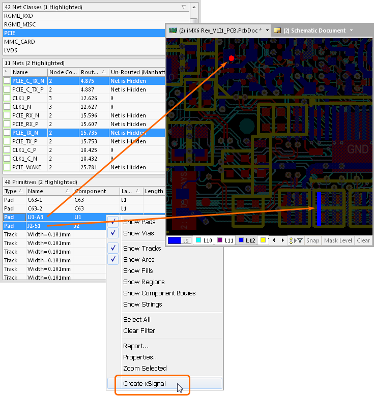
The source and destination pads (pin pairs) for the desired path are used for creating a singular xSignal definition.
The newly created xSignal will now be available in the PCB panel’s xSignals mode – its default name can be changed by selecting Properties from the right-click context menu. Note that xSignal path incorporates both nets and the series component as a single entity.
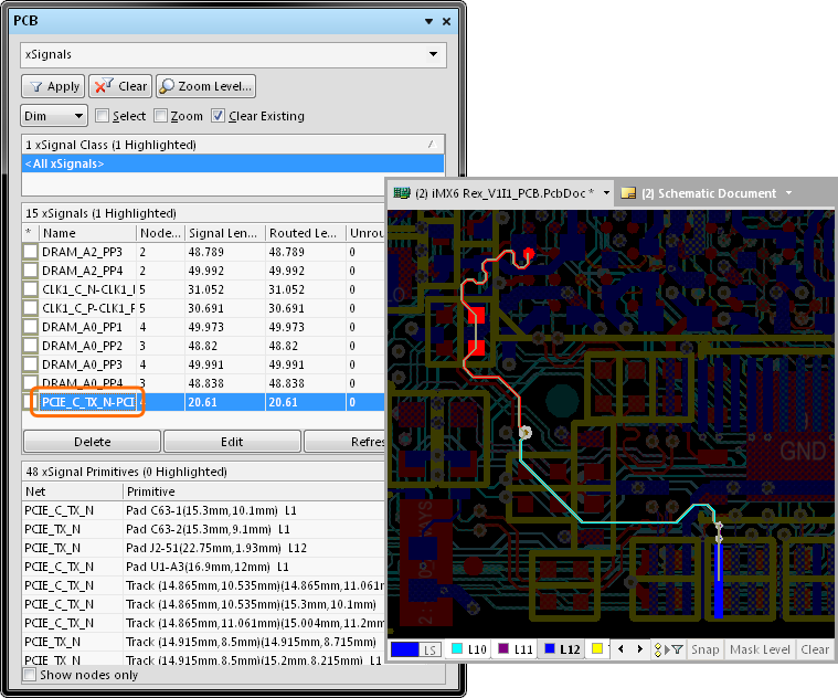
The created xSignal selected in the PCB panel and displayed in the workspace.
Browsing Components
Place the panel in Components mode by selecting Components from the drop-down list at the top of the panel. The three main list regions of the panel will change to reflect an object hierarchy, in order from the top:
- Component Classes
- Individual Components within a class
- Individual primitives that constitute a Component (pads, tracks and arcs).
The PCB panel regions allow a cumulative filter selection through component classes, to individual components, to component primitives.
Right-clicking on a component or component primitive entry and choosing the Properties command from the subsequent pop-up menu (or double-clicking on the entry directly) will provide access to the relevant properties dialog, from where you can view/modify the properties of the component/primitive as required.
Right-clicking on a component class entry and choosing Properties from the menu (or double-clicking on the entry directly) will open the Edit Component Class dialog for that class. From this dialog you can view/modify the component membership of the class, rename it, or add additional classes.
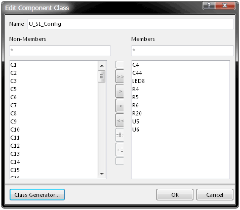
Editing a selected component class.
The display/inclusion of each component primitive type, in the Component Primitives region of the panel, is dependent on whether the corresponding option for each has been enabled on the right-click menu, accessed from either the Components or Component Primitives regions.
Right-click on a component or component primitive entry to select what items are included.
In summary, as you click on an entry in the panel's list, a filter will be applied based on that entry. The visual result of the selection (in the design editor window) is determined by the highlighting methods enabled (Mask/Dim/Normal, Select, Zoom). Multiple entries can be selected in each region, using standard SHIFT + Click and CTRL + Click features.
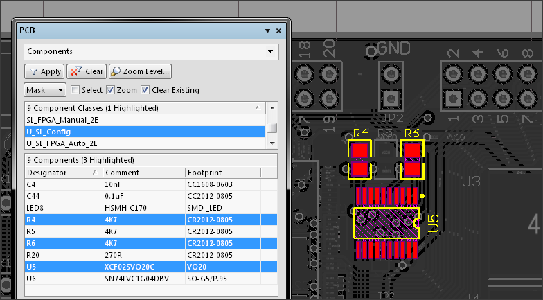
Three components are selected from the U_SL_Config component class, with the visual mode set to Mask.
Using the From-To Editor
Place the panel in From-To Editor mode by selecting From-To Editor from the drop-down list at the top of the panel. The top list section of the panel will fill with all nets currently defined for the design.
As you click on a net entry, all of the nodes on that net will be loaded into the middle list region of the panel. Filtering will be applied and a mask automatically used in order to leave just the nodes (pads) on the net fully visible, with all other objects becoming dimmed.
Selecting a net lists its nodes in the PCB panel and displays them (as pads) in the main editor workspace.
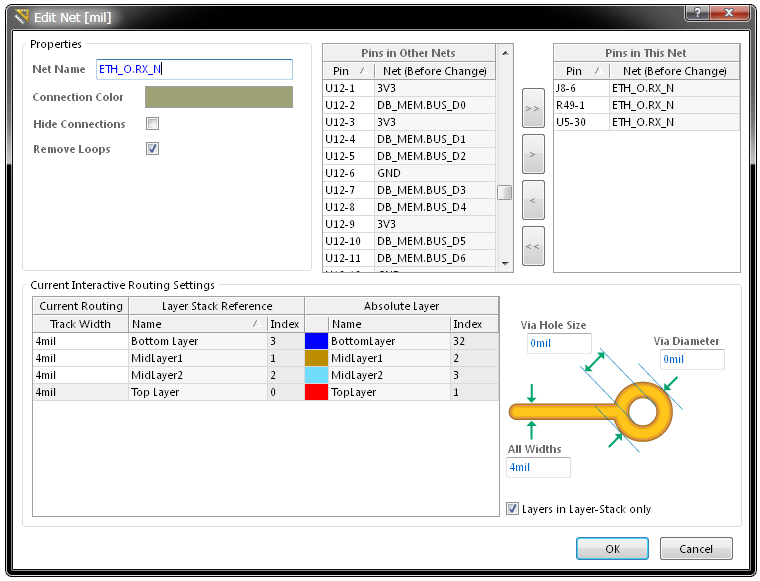
Double clicking on a net entry will open the Edit Net dialog, from where you can edit the properties of the net, including node membership.
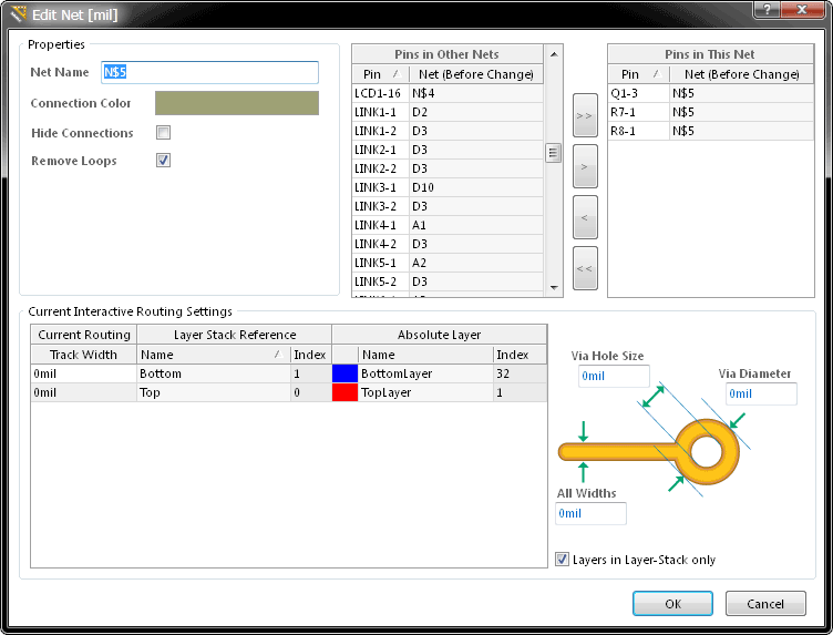
Editing the net properties in the Edits Net dialog.
Adding From-Tos
To add a user defined From-To between two nodes in a selected net, select the two nodes in the Nodes on Net region of the panel and either click the Add From To button, or right-click and choose Add From To from the subsequent pop-up menu that appears.
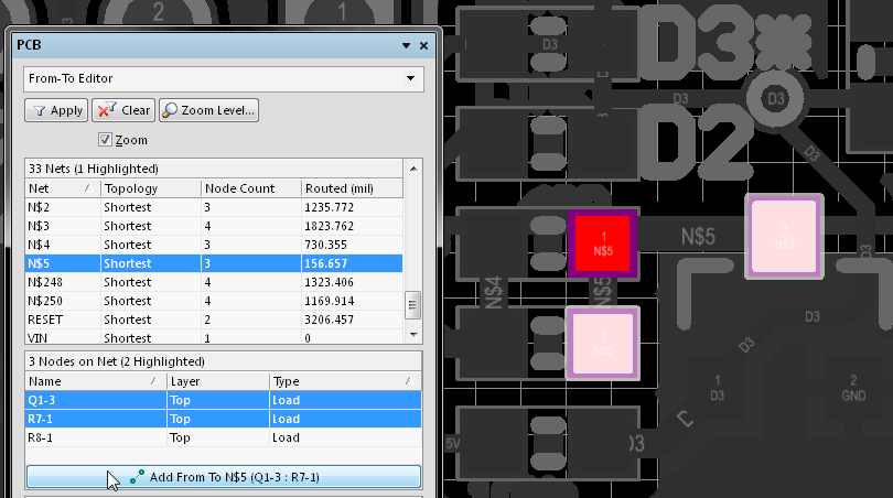
Nodes Q1-3 and R7-1 are selected, and highlighted in the workspace, so a new From-To can be defined using the Add button.
The newly added From-To will appear listed in the From-Tos on Net region of the panel and appears in the workspace as a dotted line between the two nodes.
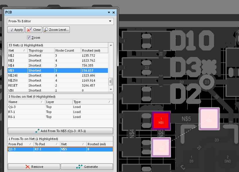
A new From-to has been created on the net, as listed in the list and graphically shown in the editor workspace.
To remove a From-To, select its entry in the From-Tos on Net region of the panel and click on the Remove button. Multiple From-Tos can be removed simultaneously. Use standard CTRL + Click and SHIFT + Click features to multi-select entries in the list.
Choosing a Predefined Topology
The topology of a net is the arrangement or pattern of the pin-to-pin connections. By default, pin-to-pin connections of each net are arranged to give the shortest overall connection length.
A topology is applied to a net for a variety of reasons; for high speed designs where signal reflections must be minimized the net is arranged with a daisy chain topology; for ground nets a star topology could be applied to ensure that all tracks come back to a common point. You can either create dedicated From-Tos for node pairs in a net, or you can choose to generate From-Tos for the net based on one of the predefined routing topologies available.
The following topologies are available and can be accessed from the From-Tos on Net region of the panel, either by clicking on the Generate button or from the right-click menu:
- Shortest - this topology connects all nodes in the net to give the shortest overall connection length
- Daisy Simple - this topology chains all the nodes together, one after the other. The order they are chained is calculated to give the shortest overall length. If a source and terminator pad are specified, then all other pads are chained between them to give the shortest possible length. If multiple sources (or terminators) are specified, they are chained together at each end
- Daisy Balanced - this topology divides all the loads into equal chains, the total number of chains equal to the number of terminators. These chains then connect to the source in a star pattern. Multiple source nodes are chained together
- Daisy Mid-Driven - this topology places the source node(s) in the center of the daisy chain, divides the loads equally and chains them off either side of the source(s). Two terminators are required, one for each end. Multiple source nodes are chained together in the center. If there are not exactly two terminators the Daisy-Simple topology is used.
![]()
- Starburst - this topology connects each node directly to the source node. If terminators are present, they are connected after each load node. Multiple source nodes are chained together, as in the Daisy Balanced topology.
A pad can be defined as a Source, Terminator or Load by changing the entry for the Electrical Type field accordingly, in the associated Pad dialog. Access to this dialog is made from within the panel by double-clicking on the entry for the pad in the Nodes on Net region.
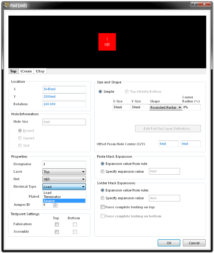
Setting a pad Electrical Type to Source in the Pad dialog.
When you change the electrical type for a pad to Source or Terminator, an "[S]" or "[T]" will be placed in the design workspace to distinguish it.

The display of the electrical type for pads and also for user-defined net topologies (displayed as dashed connection lines) are controlled via the From To Display Settings dialog, which is accessed from the Show/Hide page of the View Configurations dialog (Design » Board Layers & Colors)
After choosing a topology, the resulting From-Tos will be generated, listed in the From-Tos on Net region and subsequently added to the design workspace.
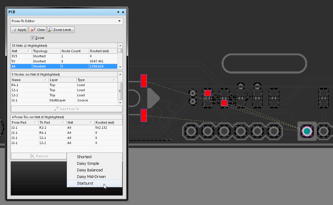
A From-To created from net A0 using the Generate button and the Starburst topology.
Using the Split Plane Editor
Note that internal planes are added to the layer stack for the design and defined using the Layer Stack Manager dialog.
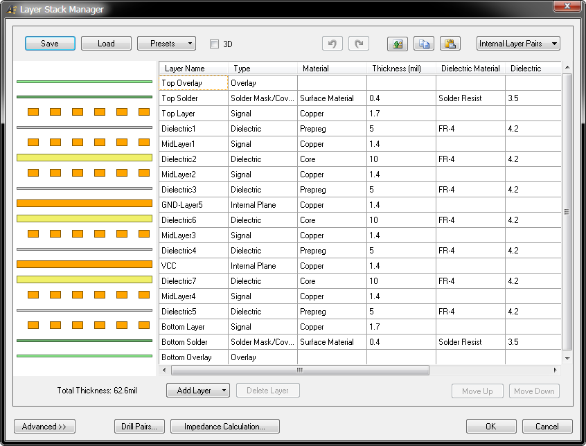
The Layer Stack Manager dialog (Design » Layer Stack Manager).
Place the panel in Split Plane Editor mode by selecting Split Plane Editor from the drop-down list at the top of the panel.
The Nets/Layers section of the panel will fill with all internal plane layers currently defined for the design. Within that section, the Split Count column indicates how many split planes exist for the corresponding plane layer. A split count of 1 effectively means that the layer has not been split, and the layer itself is considered to be a single split.
As you click on an entry in the Layers section, all of the split planes on that plane layer and their assigned nets will be loaded into the Split Planes section of the panel. To view only nets associated with split planes in this section, ensure that the Show Split Plane Nets Only option is enabled on the right-click menu. For each entry, a Node Count is displayed. This value reflects the total number of pads and vias that are connected to that split plane region.
Filtering will be applied based on the entry chosen in the Layers section, the visual result of which (in the design editor window) is determined by the highlighting methods enabled (Mask/Dim/Normal, Select, Zoom). Multiple entries can be selected using standard SHIFT + Click and CTRL + Click features.
As you click on an entry in the Split Planes section of the panel, filtering will be applied based on that entry. Again, the filtering results depend on the highlighting methods enabled and whether pads and/or vias are enabled with respect to their visibility. Multiple entries can be selected in the region.
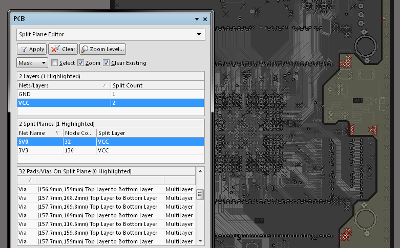
Here, the VCC layer has a 3V3 and 5V0 region split. The selected 5V0 split is visible as the highlighted region (and vias) on the right.
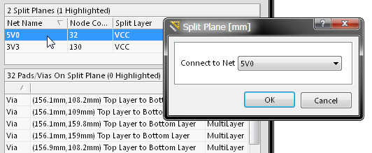
Double-click on an entry to bring up the Split Plane dialog, from where you can change the net to which the split plane region is connected. Choose from any of the currently loaded nets for the design.
The Pads/Vias On Split Plane section of the panel lists each of the pads and/or vias connecting to the split plane region chosen in the Split Planes section. Entries will only appear if the corresponding Show Pads and/or Show Vias options have been enabled from the right-click menu.
As you click on a pad or via entry, filtering will be applied based on that entry. With masking applied, the selected pad/via entry will be highlighted in the editor workspace.. If you wish to see where a pad or via resides in relation to the split plane region, click on that region within the design workspace before clicking a pad/via entry. Again, multiple entries can be chosen from the list.
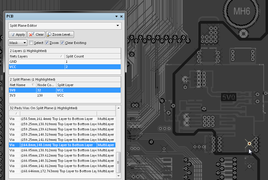
A selected Via can be seen highlighted in the board's 5V0 split plane region (shown near the mouse arrow). The VCC Layer has been selected as the editor view.
In the panel's Pads/Vias On Split Plane section, right-clicking on a pad or via entry and choosing the Properties command will open the relevant properties dialog, from where you can view/modify the properties of the pad/via as required.
Right-click a Via/Pad in the list and select Properties to open the Via/Pad Properties dialog.
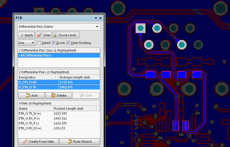
Using the Differential Pairs Editor
Place the panel in Differential Pairs Editor mode by selecting Differential Pairs Editor from the drop-down list at the top of the panel. The three main list regions of the panel will change to reflect, in order from the top:
- Differential pair classes.
- Individual member differential pairs within a class.
- The constituent nets (negative and positive) that form a differential pair.
A selected differential pair, as a member of the ETH_O class, displayed with highlighted set to Dim.
As you click on an entry in a list, a filter will be applied based on that entry, the visual result of which (in the design editor window) is determined by the highlighting methods enabled (Mask/Dim/Normal, Select, Zoom). In this way you can quickly highlight all differential pairs in a particular class, a particular differential pair, or a particular net that forms the negative or positive half of a differential pair. Multiple entries can be selected in each region, using standard SHIFT + Click and CTRL + Click features.
Right-clicking on a differential pair class entry and selecting Properties (or double-clicking on the entry directly) will open the Edit Class dialog, where you can rename it or view/modify the differential pair membership of the class. For full control and editing of all classes, including Differential Pair Classes, open the Object Class Explorer dialog through the Design » Classes menu path.
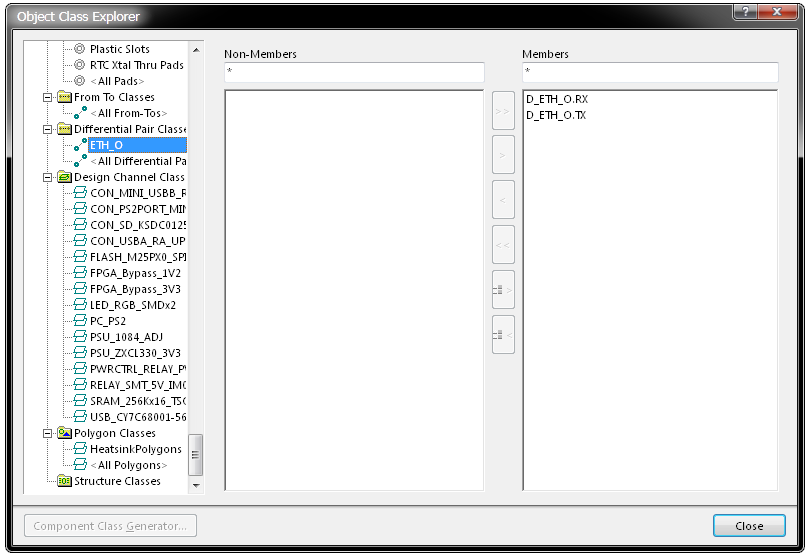
The Object Class Explorer allows creating, viewing and modification for all classes, including Differential Pairs.
Right-clicking on a Differential Pair entry in the PCB panel and selecting Properties (or double-clicking on the entry directly) will provide access to the Differential Pair dialog, from where you can view/modify the properties for differential pair name and its constituent nets. See the following Managing Differential Pairs section for more on the Differential Pair dialog.
Right-clicking on a net entry in the PCB panel and selecting Properties (or double-clicking on the entry directly) will provide access to the Edit Net dialog, from where you can view/modify the properties of the net as required.
Back in the PCB panel, as you click on an entry in a list a filter will be applied based on that entry. The visual result (in the design editor window) of the cumulative filter is determined by the highlighting methods enabled (Mask/Dim/Normal, Select, Zoom).
In this way you can quickly highlight all differential pairs in a particular class, a particular differential pair, or a particular net that forms the negative or positive half of a differential pair. Multiple entries can be selected in each region, using standard SHIFT + Click and CTRL + Click features.
Managing Differential Pairs
Use the Differential Pairs region of the panel to manage the differential pair objects in a design. For the particular differential pair class selected, all currently defined differential pair objects that belong to that class will be listed in this region.
Use the buttons at the bottom of this region to create new differential pair objects, or edit or delete existing ones. These three commands are also available from the right-click menu for the region. When adding a new differential pair, the Differential Pair dialog will open.
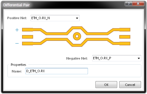
Use the dialog to define the pair object, in terms of a positive and negative net and a meaningful name. By default, the name will be set to NewDifferentialPair1 and the positive and negative nets will be set to the first and second available nets in the netlist for the design. Use the drop-down lists to select from the available nets.
When editing an existing differential pair object, the Differential Pair dialog will again appear, with the currently chosen nets for the pair entered into the Positive Net and Negative Net dropdown fields respectively. Change one or both nets for the pair, or rename the pair, as required.
Creating Differential Pairs from Design Nets
Differential pair objects can be automatically created from the nets in your design using the Create Differential Pairs From Nets dialog. This dialog is accessed by clicking on the Create From Nets button at the bottom of the Nets region of the PCB panel.
Prospective differential pair objects are listed for creation in response to the filter entries at the top of the dialog.
The effectiveness of this automated method directly depends on the naming convention that has been used for the specific nets that will make up the differential pairs. Ideally, a naming convention will be used whereby a common root is followed by a consistent positive/negative indicator (P and N). For example, consider the receiver signal D_ETH_O.RX (see above), which is a differential signal in the design. The two nets that constitute this signal are ETH_O.RX_P and ETH_O.RX_N - these represent the positive and negative sides of the signal, respectively.
The filters at the top of the dialog enable you to quickly target these nets in terms of the net class to which they belong and the particular differentiating factor that has been used to distinguish the positive and negative nets in an intended pairing - for example, _P and _N. You can also define a prefix to be added to the differential pair objects created, and also determine in which differential pair class they are to be added. In the above example, notice that the name for a differential pair object is created using the prefix specified and the root of the differential pair signal. The polarity indicators are discarded.
For each differential pair object, the dialog lists its constituent positive and negative nets. By default, all prospective differential pair objects are selected for creation, and individual ones can be excluded by clearing the associated Create check box. In the example above, only D_ETH_O.RX is checked for creation.
When all options are set as required, click the Execute button - the differential pair objects will be created and the PCB panel will update accordingly.
Filtering will be applied to show the created pairs in the workspace, as shown below.
Differential pair objects created from nets. In practice, differential pairs would normally be defined before the nets are routed.
Configuring Applicable Design Rules
A Differential Pair Routing rule needs to be configured before routing a differential pair in a design. A differential routing rule defines:
- The preferred Gap between the network pair, and its permitted range.
- The maximum Uncoupled Length (the pair is uncoupled when the gap is wider than the maximum Gap setting).
- The preferred routing Width for each net.
- The optional gap/width setting variations for each layer in the stack.
- The scope (in terms of classes and objects) for the rule's application.
While rules can be created manually using the PCB Rules and Constraints Editor (Design » Rules), the PCB panel offers the convenience of the Differential Pair Rule Wizard. Use the Rule Wizard button (below the Nets region in the PCB panel) to access the Wizard and implement the rule properties as required.
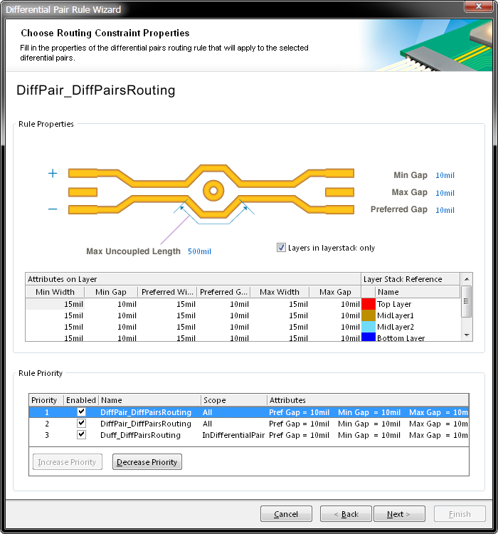
The Differential Pair Rule Wizard guides you through the rule definition process.
Note that the scope of the rules will depend on the selection in the PCB panel prior to launching the wizard, as follows:
Differential Pair Class
If the All Differential Pairs class is selected, the scope will be All for each rule.
If a specific differential pair class is selected, the scope will be InDifferentialPairClass('ClassName') for each rule.
Differential Pair
If a single differential pair object is selected in the panel, the scopes will be:
- Width -
InDifferentialPair('PairName') - Matched Net Lengths and Differential Pairs Routing -
IsDifferentialPair And (Name = 'PairName'))
If multiple differential pair objects are selected in the panel, there will be individual scope entries for each pair object, each separated by an Or operator. For example a routing Width rule targeting individually selected differential pair objects D_ETH_O.TX and D_ETH_O.RX will have a scope of:
InDifferentialPair('D_ETH_O.TX') Or InDifferentialPair('D_ETH_O.RX')
To edit the configuration of an existing Differential Pairs Routing rule, including its scope etc, open the PCB Rules and Constraints Editor dialog (Design » Rules from the main menu) and navigate to Routing - Differential Pairs Routing.
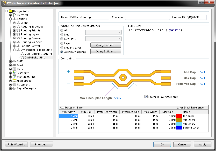
For a differential pair the Gap settings can either be set for all layers using the controls beside the image of the pairs, or they can be set for each layer in the grid region below the image.
Browsing Polygons
Place the panel in Polygons mode by selecting Polygons from the drop-down list at the top of the panel. The three main list regions of the panel will change to reflect, in order from the top:
- Polygon Classes.
- Individual Polygons within a class.
- Individual primitives that constitute a Polygon (tracks, arcs and regions).
For full control and editing of Polygon Classes, open the Object Class Explorer dialog through the Design » Classes menu path. From this dialog you can view/modify the polygon membership of the class, rename it, or add additional classes.
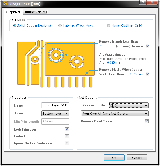
In the PCB panel, right-clicking on a polygon entry and selecting Properties (or double-clicking on the entry directly) will open the Polygon Pour dialog, from where you can view/modify the Polygon properties as required.
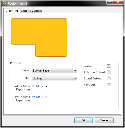
Similarly, right-clicking on a polygon primitive entry and selecting Properties (or double-clicking on the entry directly) will provide access to the relevant properties dialog, such as the Regions dialog, from where you can view/modify the properties of the primitive as required.
In the PCB panel's Polygon Primitives region, the display/inclusion of each polygon primitive type is dependent on the setting of corresponding enabling option, accessed from right-click menu.
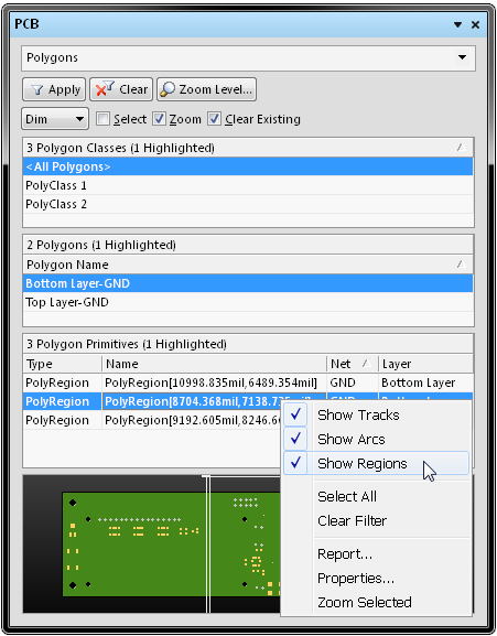
As you click on an entry in the PCB panel's list a filter will be applied based on that entry, where the visual result of which (in the design editor window) is determined by the enabled highlighting methods (Mask/Dim/Normal, Select, Zoom). Multiple entries can be selected in each region, using standard SHIFT + Click and CTRL + Click features.
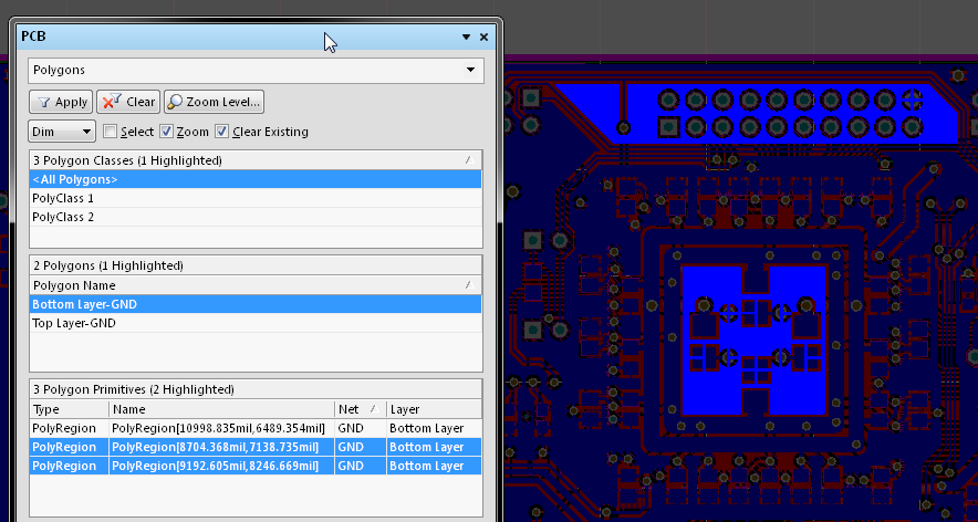
Polygons are formed by multiple primitives such as tracks, arcs and regions. Two regions are selected above, and the PCB view set to Dim.
Using the Hole Size Editor
Place the PCB panel in Hole Size Editor mode by selecting Hole Size Editor from the drop-down list at the top of the panel. The three main list regions of the panel will change to reflect, in order from the top:
- The general filtering for hole types and their status.
- Hole objects arranged in groups, as determined by size and shape.
- Individual primitives that constitute each group of hole objects (pads, vias and slots).
The three panel sections show the cumulative filtering applied to hole types, styles and status.
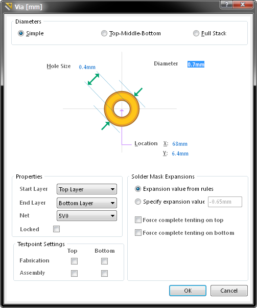
The groups of holes can be collectively edited in the Unique Holes section of the panel by entering values in the appropriate column cell. You can enter a value in mm to change the current hole size for pads and vias in the Hole Size column.
Editing the hole size for the selected group of six matching hole styles.
You can also change the corresponding Length, Type and Plated entries for holes where applicable.
Changing the hole type (from round to square) for the selected group of six matching hole styles.
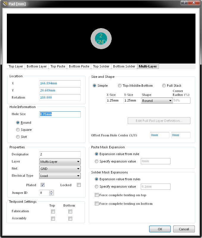
Individual pad/via objects belonging to the selected holes group are listed in the lower Pad/Via section of the PCB panel. Right-clicking on an object in the list and selecting Properties (or double-clicking on the entry directly) will open the matching dialog for that primitive, where its properties can be viewed and edited.
As you click on an entry in the PCB panel's lists a cumulative filter will be applied based on that entry. The visual result of this (in the design editor window) is determined by the highlighting methods enabled (Mask/Dim/Normal, Select, Zoom). In this way you can quickly highlight all holes of a particular status, holes of a particular style or size, or an individual hole primitive (pad/via) that exits in that filtered group. Multiple entries can be selected in each list section, using standard SHIFT + Click and CTRL + Click features.
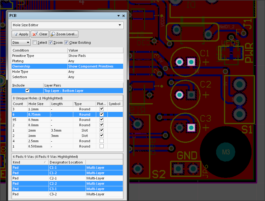
The panel selections filter down to hole primitives of a specific type. Four are selected and displayed here from the '0.75mm & Round' group, as selected above.
Browsing 3D Models
Place the PCB panel in 3D Models mode by selecting 3D Models from the drop-down list at the top of the panel. Change to 3D viewing mode through the View » Switch to 3D menu, or use the '3' shortcut.
The three main list regions of the panel when in 3D Model mode reflect, in order from the top:
- Component classes.
- Specific components associated with the component class that have associated 3D body object(s) or free models (non-PCB mounted, free-floating 3D bodies).
- The individual 3D bodies for each component or free model.
The PCB panel's filter scope progresses through component classes to components and their constituent model elements, while the visual result tracks the changes.
As you click on a specific component in the Components region of the panel, filtering will be applied using the component as the scope of the filter. The visual result (in the design editor window) is determined by the highlighting methods enabled (Mask/Dim/Normal, Select, Zoom). Multiple rule entries can be selected using standard SHIFT + Click and CTRL + Click features.
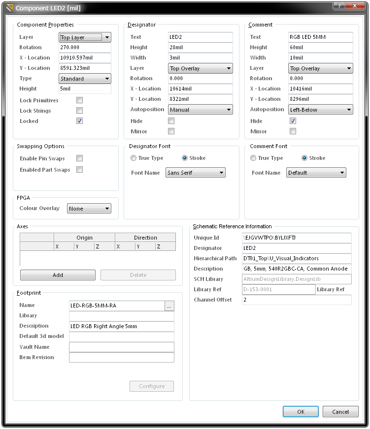
Double-clicking a component entry in the Component region of the panel (or right-clicking and choosing Properties) will open the relevant Component dialog, from where you can edit its properties in detail.
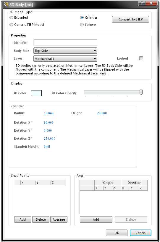
Similarly, double-clicking a model entry in the Models region of the panel (or right-clicking and choosing Properties) will open the relevant 3D Body dialog, from where you can edit the complete 3D body properties.
When selecting a component's constituent models from the Models list area in the PCB panel, the view in the editor workspace will zoom, dim/mask or select accordingly.
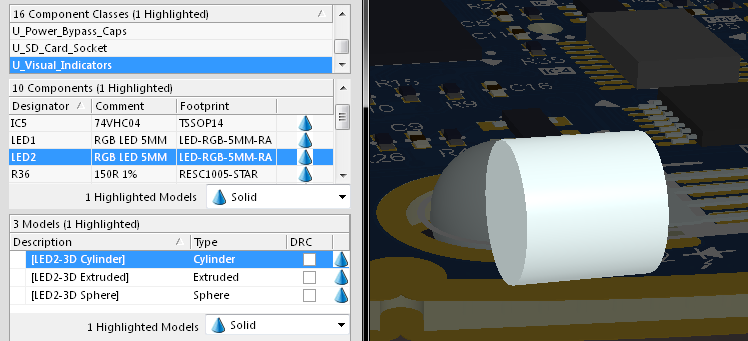
An individual model selected from a component. In this case, a cylinder from a LED component in the board's U_Visual_Indicators class.
The PCB panel can be used to select display properties for 3D models. The cone icons ![]() represent different levels of transparency from 100% (hidden) down to 0% (solid) in increments of 25%. You can select multiple components and apply the same display controls to them at once using the Highlighted Models options.
represent different levels of transparency from 100% (hidden) down to 0% (solid) in increments of 25%. You can select multiple components and apply the same display controls to them at once using the Highlighted Models options.
The selected cylinder model being set to 75% opacity. Multiple models can also be selected and changed in one step.
Multiple Model entries can be selected using standard SHIFT + Click and CTRL + Click features, providing full control over the 3D Model view and the base 3D elements that make up a component.
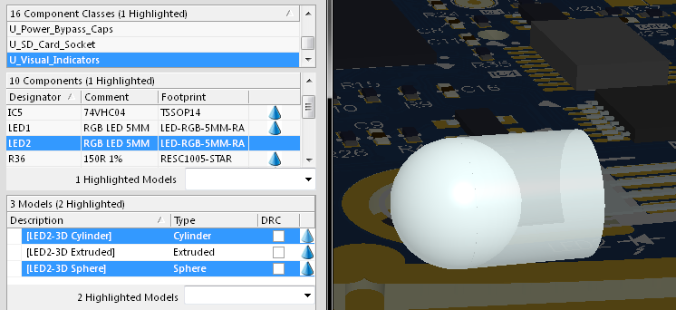
Here, both a cylinder (set to 75% opacity) and a sphere (solid / 0% opacity) from a LED component are selected.
Browsing Layer Stack Regions
Place the PCB panel in Layer Stack Regions mode by selecting Layer Stack Regions from the drop-down list at the top of the panel. Change to the Board Planning Mode view through the View » Board Planning Mode menu, or use the 1 shortcut.
A Layer Stack Region is a user-defined area of a PCB that can have a unique layer stack assigned to it. A board can split into multiple regions, with each region assigned an individual layer stack arrangement. The layer stackups (defined in the Layer Stack Manager dialog) can be configured to cater for both rigid and flexible regions of the board, facilitating rigid-flex PCB design.
The three main list regions of the panel when in Layer Stack regions mode reflect, in order from the top:
- The names of the available Layer Stacks.
- The Stackup Regions defined on the board, or those assigned to a selected Layer Stack.
- The list of Bending Lines in the selected Stackup Region
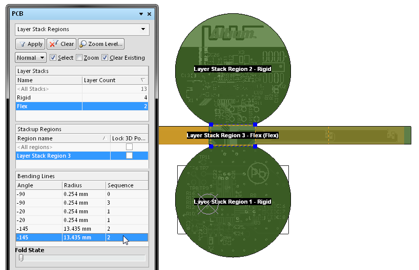
A board can split into distinct regions (Stackup Regions) that are assigned specific layer stackup arrangements (Layer Stacks). Folding areas (Bending Lines) are defined in the board's flexible regions.
When a particular layer stackup name is selected in the Layer Stacks area of the PCB panel, filtering will be applied using the Layer Stack as the scope of the filter. Any board regions assigned to that stackup will therefore be listed in the panel's Stackup Regions area. In turn, any bend lines defined in a selected Stackup Region will be listed in the Bending Lines list area.
Double clicking on a Stackup Region in the list (or double clicking on the board region itself in the design workspace) opens the Board Region properties dialog. Use this dialog to rename a region, assign it to a layer stack or lock its 3D properties.
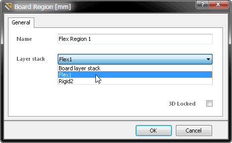
A board region's name (Flex Region 1) and its assigned layer stackup (Flex1) defined in the Board Region dialog. One region should be locked as a 3D reference.
Double clicking on a Bending Line in the panel's Bending Line area list opens the Bending Line dialog, from where the line's properties can be edited in detail.
The Bending Line properties have interrelated values where the Affected area width is calculated from the Bending Angle and the Radius. So when the first two properties are edited in the dialog for example (the Radius and the Bending Angle), the third property (area width) will be calculated automatically. Note that each Bending Line's Affected area width is displayed on the board in dark yellow.
The Fold Index defines the sequence that the bends are folded when the Fold State slider or View » Fold/Unfold command is used. The slider is just below the Bending Lines area in the panel – use it to fold the board up in 3D mode (shortcut 3).
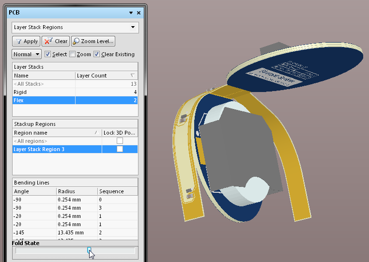
The board in 3D view, part way through its fold up range as set by the position of Foldup State slider.
See Defining Board Regions and Bending Lines for more information on flexible board regions and defining their properties.
Right-Click Menus
The following is a summary of all right-click menu commands that can appear for the panel. The actual content of the menu varies, depending on the current mode of the panel and the particular region of the panel from where the menu is accessed:
- Select All - quickly select all entries in the section of the panel from which the right-click menu was accessed
- Clear Filter - clear the currently-applied filter. All objects in the design workspace will become fully visible and available for selection/editing
- Report - generate a report in context with the section of the panel the menu is accessed from. After launching the command, the Report Preview dialog will appear from where you can peruse, print and export the report in various file formats
- Properties - access the corresponding properties dialog for the chosen object, from where you can view/modify the properties for that object. For example, with a component entry selected, using this command will access the associated Component dialog. If a specific rule entry is selected, using this command will bring up the associated Edit PCB Rule dialog, and so on
- Show Pads - enable to display pad entries in the relevant list section of the panel. For example, to display pad entries in the Component Primitives section when in Components mode, or in the Pads/Vias On Split Plane section, when in Split Plane Editor mode
- Show Vias - enable to display via entries in the relevant list section of the panel. For example, to display via entries in the Net Items section when in Nets mode, or in the Pads/Vias On Split Plane section, when in Split Plane Editor mode
- Show Tracks - enable to display track entries in the relevant list section of the panel. For example, to display track entries in the Net Items section when in Nets mode
- Show Arcs - enable to display arc entries in the relevant list section of the panel. For example, to display arc entries in the Component Primitives section when in Components mode
- Show Fills - enable to display fill entries in the relevant list section of the panel. For example, to display fill entries in the Net Items section when in Nets mode
- Show Regions - enable to display region entries in the relevant list section of the panel. For example, to display region entries in the Net Items section when in Nets mode
- Show 3D Bodies - enable to display 3D body entries in the relevant list section of the panel. For example, to display 3D body entries in the Component Primitives section when in Components mode
- Show Strings - enable to display string entries in the relevant list section of the panel. For example, to display string entries in the Net Items section when in Nets mode
- Loop Removal - use the commands available on this sub-menu to set the Loop Removal attribute for nets as required, in the Nets section of the panel when in Nets mode. You can choose to enable/disable the attribute for all or selected nets. You can also toggle the attribute's status for all or selected nets. With the attribute enabled, redundant loops will automatically be removed as you interactively route a net, provided the Allow Automatic Loop Removal option is enabled on the PCBEditor - General page of the Preferences dialog
- Add From To - create a From-To between two chosen pad entries in the Nodes on Net section of the panel, when in From-To Editor mode
- Remove - remove the From-To chosen in the From-Tos on Net section of the panel, when in From-To Editor mode
- Shortest - apply the Shortest topology to the chosen net, when in From-To Editor mode
- Daisy Simple - apply the Daisy Simple topology to the chosen net, when in From-To Editor mode
- Daisy Balanced - apply the Daisy Balanced topology to the chosen net, when in From-To Editor mode
- Daisy Mid-Driven - apply the Daisy Mid-Driven topology to the chosen net, when in From-To Editor mode
- Starburst - apply the Starburst topology to the chosen net, when in From-To Editor mode
- Show Split Plane Nets Only - enable to display only nets connecting to split plane regions, in the Split Planes And Nets section of the panel, when in Split Plane Editor mode
Notes
- With the Mask or Dim option selected, clicking on a rule entry will allow you to accurately examine which objects the enabled rule applies to and can be a great aide when creating your query for the rule scope(s). Because you can edit a rule directly from the panel, you can tweak your query until the desired objects are captured by the scope.
- CTRL + Click over a selected entry to deselect it. If the entry is the only one selected for that region, performing this action will clear the filter.
- The entries for the All Nets, All Components and All Differential Pairs classes cannot be modified or deleted in the Object Class Explorer dialog.
- In sections of the panel where multiple columns of data exist, the data may be sorted by any column by clicking on the header for that column. Clicking once will sort in ascending order. Click again to sort by descending order.
- You can change the order in which columns of data are displayed. To move a column, click on its header and drag it horizontally to the required position. A valid position is indicated by the appearance of two green positional arrows.
- Filtering applied when using Queries from the PCB panel is permanent for the current session. A permanent filter must be cleared by clicking on a corresponding Clear button (e.g. at the bottom-right of the design editor window) or by applying an empty query from the PCB panel.