JTAG Viewer
Contents
The following content has been imported from Legacy Help systems and is in the process of being checked for accuracy.
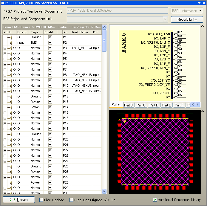
The Pin State Panel shows the configuration of every pin, and can also show the current pin activity.
Function
The pin states panel associated with a physical FPGA device provides information concerning the mapping of interface ports in the source FPGA design to the physical pins of the FPGA device in which the design is running. You can also monitor the state of all physical pins of the associated FPGA device, in real time.
Content and Use
The main area of the panel provides mapping information between the pins of the physical FPGA device and the top-level ports of the associated FPGA design project.
Entries for each pin of the physical device are listed in terms of pin direction and type. For all non-power pins, the associated Boundary Scan cell information is also included. This information can be accessed by clicking on the expand symbol next to the pin entry, or by double-clicking anywhere within the row for that entry.

Expand the pin detail to display BSDL information.
Note that for single direction pins (input or output) there will be a single cell used. For IO pins, three cells are used - one for input, one for output and one used as a control to configure direction.
Where a device pin has been assigned for use within the FPGA design (through definition of the relevant constraint file), the entry for the pin will show the corresponding interface port in the design and the direction of this port. The field at the bottom right of the panel displays the name of the top-level document upon which these ports can be found.
Pin to Port mapping is shown on the top level schematic sheet.
Enable the Hide Unassigned I/O Pins option at the bottom of the panel to display only those pins of the physical device that are actually assigned and used by the programmed FPGA design.
Real-time monitoring of FPGA pins
The state of all physical pins of the device can be monitored in real time, by enabling the Live Update option (at the bottom of the panel). With this feature enabled, a column of LEDs is displayed in the panel - one LED per physical pin.
Pin activity can be monitored by enabling the Live Update option.
As you interact with the design, affected pins will toggle state, which is reflected in the auto-updated state of the corresponding LEDs in the panel.
You can manually update the pin statuses at any time by clicking the Update button:
Accessing BSDL Information
If you are using a physical device that is not supported by the system, the device will appear in the Hard Devices chain of the Devices view as a Generic JTAG Device.
In this case no specific Nexus driver exists for the device (no .NEX file in the \System folder of the installation). To get the system to drive a Hard Devices chain containing such a device, you will need to attach a Boundary Scan Description Language (BSDL) file for the specific device you are using. Such files can be obtained from the relevant vendor website. Once attached, the system will use the information in the file - including the device's ID Code and Instruction Register Length - to correctly configure the Hard Devices chain.
In the associated pin states panel for the physical device, you can click on the BSDL Information button to access data contained in the BSDL file that you have attached.
Notes
- The pin states panel for a physical device is accessed by clicking the Show Pins Panel button on the associated instrument panel for that device. The latter is loaded into the Instrument Rack - Hard Devices panel upon double-clicking on the entry for the device, in the Hard Devices chain of the Devices view.
- Mapping information may be sorted by any column by clicking on the header for that column. Clicking once will sort in ascending order. Click again to sort by descending order.
- You can change the order in which columns of data are displayed. To move a column, click on its header and drag it horizontally to the required position. A valid position is indicated by the appearance of two green positional arrows.
- Direct filtering is available, allowing you to quickly jump to a pin entry by directly typing within the panel. You can filter based on any data column in the panel. Use the Right Arrow and Left Arrow keys to switch between columns for filtering, or click directly on a field within a column. To use this feature, click within a data column and type the first letter of the entry you wish to jump to. The first entry in that column starting with the letter you type will become selected and the letter will be highlighted to show that filtering of the column content is based upon it, as illustrated in the example below:
If the data column contains multiple entries starting with the same letter, narrow your search by typing additional letters as required.
To clear the current filtering, allowing you to enter a different starting letter, press ESC. Use the BACKSPACE key to clear the previously entered filter characters, in sequence.
As you switch between data columns for filtering purposes, the current filter is cleared. - The status of FPGA device pins can also be monitored directly from the schematic sheet by placing a probe directive on any net that connects to an FPGA pin, as illustrated in the image below.
Note that for this feature to function, the source FPGA design must be downloaded to the physical FPGA device and the associated pin states panel for the device must be open and remain open. - A BSDL file is attached to a Generic Device by right-clicking on the icon for the device in the Hard Devices chain of the Devices view and choosing the Attach BSDL File command. The Set Generic Device BSDL File Path dialog will appear. By default, the path is set to the Library\BSDL\Generic folder of your Altium Designer installation. BSDL files should be placed in this folder and a reference to each entered into the BSDL_FileMap.Txt file, which is also located in this folder.