PCB Editor
The following content has been imported from Legacy Help systems and is in the process of being checked for accuracy.
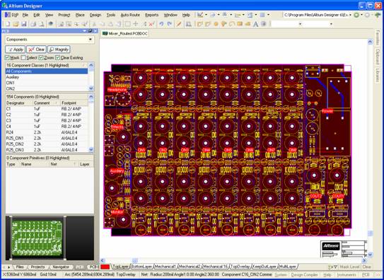
The PCB Editor allows you to create, edit and verify the PCB design, as well as generate the output files required to manufacture the printed circuit board. This comprehensive reference provides information on the editing capabilities of the PCB Editor to help you layout your PCB design.
Contents
- Editor Environment
- Specifying Board Options
- View Configurations
- Specifying Workspace Preferences
- Right-click Menus
- Panning
- Zooming
- Rotation (3D Mode)
- Moving a Group of Selected Objects
- Moving a Group of Selected Components Sequentially
- Changing the Current Layer
- Selection Memory
- Mask Level Controls
- Clear Filtering
- TrueType Font Support
- Associated Panels
- Associated Design Objects
- Design Rules
- Re-entrant Editing
Editor Environment
When the PCB Editor is active (i.e. a PCB document (*.PcbDoc) is open and active) the main application window will contain:
- a main design window in which to design - capable of display in 2D and 3D modes. 2D mode has a larger feature set as the majority of board design is carried out more naturally in a 2D model space. View settings for any project can be saved as a "view configuration" and used time and again.
- editor-specific menus and toolbars
- workspace panels - both global and editor-specific.
Object placement, routing and graphical editing is carried out on the PCB document which, when opened, appears as a tabbed document view in the main design window.

The use of the main design window in terms of actual design (placement, editing, routing, design rule checking, etc) is outside the scope of this topic and information for such should be sought in the relevant documentation. The following sections, however, offer useful hints and tips with respect to the main design workspace in general.
Specifying Board Options
Options specific to the active PCB document are defined in the Board Options dialog, which can be accessed by selecting Design » Board Options.
![]()
![]()
![]()
This dialog provides controls for defining the various grid systems, specifying units of measurement and controlling the display and position of an associated (back) sheet on which the board is placed.
Note : Many dialogs feature a units toggle control ![]() in the top-left corner that will change the units of measurement currently used in the dialog between metric and imperial [shortcut: CTRL + Q ]. The current unit of measurement is displayed in the dialog title area. Toggling units at any time does not affect system accuracy as all numerical calculations are carried out at system resolution. The workspace Preferences dialog ( DXP » Preferences ) can also be used to control the display precision and rounding of metric units between three and five digits to the right of the decimal point.
in the top-left corner that will change the units of measurement currently used in the dialog between metric and imperial [shortcut: CTRL + Q ]. The current unit of measurement is displayed in the dialog title area. Toggling units at any time does not affect system accuracy as all numerical calculations are carried out at system resolution. The workspace Preferences dialog ( DXP » Preferences ) can also be used to control the display precision and rounding of metric units between three and five digits to the right of the decimal point.
To define the layer stack for the active PCB document, select Design » Layer Stack Manager. The Layer Stack Manager dialog will appear.
View Configurations
The PCB Editor can display the PCB model in 2D or 3D modes with definitions for layers, surfaces, 3D colors, visibility and other items, known as view configurations, available from the View Configurations dialog. You can save any 2D or 3D view configurations for use time and again. Select Design » Board Layers & Colors [shortcut: L] to display the View Configurations dialog.
2D mode is a multi-layered environment that is ideal for normal PCB design routines such as placing components, routing and connecting. 3D mode is useful for examining your design both inside and out as a full 3D model (3D mode does not provide the full range of editing functionality available in 2D mode). You can switch between 2D and 3D modes through File » Switch To 3D or File » Switch To 2D [shortcut: 2 (2D), 3 (3D)].
Note : 2D layer and system colors edited via the View Configurations dialog are system-based. Ie, they will be applied to all PCB documents, similarly to editing them via the Preferences dialog.
In each case, use the dialog's 'What's This Help' feature to obtain detailed information about each of the options available. Click on the question mark button at the top right of the dialog and then click over a field or option to pop-up information specific to that field or option.
Specifying Workspace Preferences
General workspace preferences - applicable to all PCB documents - are defined on the relevant pages contained within the PCB Editor section of the Preferences dialog. Select Tools » Preferences to display the PCB Editor - General page of this dialog.
Again, use the dialog's 'What's This Help' feature to obtain detailed information about each of the options available across the various pages.
Right-click Menus
Right-clicking in the main design window will open a [pop-up] menu providing commands to access commonly used features, such as document options and workspace preferences, as well as commands that are in context with the object currently under the cursor.
Panning
Panning in the workspace can be carried out in the following ways:
- using the horizontal and vertical scroll bars
- using the keyboard arrow keys (holding SHIFT key for faster movement)
- using mouse-wheel for up/down, SHIFT + Mouse-wheel for left/right
- right-drag mouse to pan in any direction.
Zooming
Zooming in the workspace can be achieved in the following ways:
- CTRL + Right-drag mouse or CTRL + Mouse-wheel or PAGE UP / PAGE DOWN keys
- using the PAGE UP (zoom in) and PAGE DOWN (zoom out) keyboard shortcuts. (Hold down the SHIFT and CTRL keys to provide finer and coarser zooming respectively)
- using the mouse-wheel (push the mouse-wheel button down and move mouse).
Rotation (3D Mode)
Hold down SHIFT to enter 3D rotation mode. This is represented on screen as a directional sphere at the cursor position. Rotational movement of the model is made about the center of the sphere using the following controls:
- Right-drag sphere Center Dot with the mouse for full floating view - rotate in any direction.
- Right-drag sphere Horizontal Arrow with the mouse to rotate the view about the Y-axis.
- Right-drag sphere Vertical Arrow with the mouse to rotate the view about the X-axis.
- Right-drag sphere Circle Segment with the mouse to rotate the view in the Y-plane.
Note : Altium Designer supports a number of 3D mouse and 3D space navigation devices. These devices can improve the 3D navigation experience.
Moving a Group of Selected Objects
You can move selected objects using a combination of the CTRL key and arrow keys (vertically or horizontally), the CTRL and SHIFT keys and arrow keys, or freely using the mouse, on the PCB document.
When using the keyboard to reposition selected objects, the distances are set according to the current Snap Grid setting in the Board Options dialog (Design » Board Options or shortcut D, O). Use this dialog to change the Snap Grid X (horizontal) and Y (vertical) values. This Grid value also appears on the Status bar of Altium Designer. Use the G shortcut to cycle through different snap grid setting values. You can also use the View » Grids submenu or the Snap Grid right-click menu.
- Selected objects can be 'nudged' by small amounts (according to the current snap grid value) by pressing the arrow keys while holding down the CTRL key.
- Selected objects can also be 'nudged' by large amounts (snap grid value by a factor of 10) by pressing the arrow keys while holding down the CTRL and SHIFT keys together.
Moving a Group of Selected Components Sequentially
You can reposition a number of selected components sequentially in the order that you selected them.
You need to select the components you want to move one at a time using SHIFT + Click on each.
Once your components are selected, select the Tools » Component Placement » Reposition Selected Components command. The cursor appears as a crosshair with the first selected component attached to it. Reposition the component by clicking at the new position (normal cursor snap movement and free mouse movement are available).
Once component placement is finished, all the originally selected components will remain selected. Click anywhere in the workspace to exit sequential component placement mode.
Changing the Current Layer
One workspace layer is current at any given time. Some design objects, such as tracks, fills, text or single layer pads are placed on the current layer. Other design objects, such as components, multi-layer pads and vias, can be placed without regard to the current layer. Selection (for moving, deleting, etc) is layer-independent - you can perform these operations on any primitives without having to change the current layer.
At the bottom of the main design window there is a color-coded tab for each layer that is enabled with respect to its visibility in the workspace (from the View Configurations dialog).
![]()
The currently selected layer name is shown bolded for easy identification. A layer can be made current by clicking on its corresponding tab. Alternatively use the + and - keys on the numeric keypad to cycle forward and backward through all enabled layers in the workspace. Pressing the * key on the numeric keypad cycles through enabled signal layers. Use layer tabs as follows:
- Click selects the layer
- CTRL + Click selects the layer and highlights layer content
- CTRL + ALT + Cursor-hover selects the layer and highlights its content
- CTRL + SHIFT + Click selects the layer and toggles highlighting
- Right-click for pop-up menu with commonly-used layer-related commands including layer visibility.
The color assigned to each layer is indicated by the color swatch on the left of each layer tab.
Selection Memory
The Selection Memory feature enables you to select objects in your design and save the selection for recall at any time. You can reselect the objects directly via the Selection Memory dialog. Selections are saved with the PCB document.
Click the ![]() button at the bottom right of the main design window to access the Selection Memory dialog. This dialog provides full control over the selection memory feature.
button at the bottom right of the main design window to access the Selection Memory dialog. This dialog provides full control over the selection memory feature.
Mask Level Controls
Click the Mask Level button at the bottom right of the main design window to access a pop-up containing controls for adjusting the masking level when the mask highlight method is employed as part of temporary or permanent filtering, eg. when applying a query from the PCB Filter panel, when browsing design objects using the PCB panel, or when interactively routing. The effectiveness of masking and dimming is determined by the Highlighting Options set in the PCB Editor - Display page of the Preferences dialog.
When Mask is enabled, filtered objects will appear visible in the design editor window, with all other objects being made monochrome. The Masked Objects Factor slide control determines the level of shade applied to unfiltered objects, the Background Objects Factor slide control determines the level of visibility of unfiltered objects.
When Dim is enabled, filtered objects will appear visible in the design editor window, with all other objects retaining their colors, but being shaded. There are two controls to set the contrast between filtered and unfiltered objects. The Masked Objects Factor slide control determines the level of shade applied to unfiltered objects, the Highlight Objects Factor determines how white the filtered objects highlight is.
Clear Filtering
Click the Clear button at the bottom right of the main design window, or use the SHIFT + C keyboard shortcut, to clear any existing filtering applied to the current PCB document. If the filtering is temporary in nature, click anywhere inside the main design window to clear it. If the filtering is permanent in nature, you must use the Clear button, or one of its counterparts which can be found in the respective dialog(s) or panel(s) from which the original filtering was initiated.
TrueType Font Support
The PCB Editor offers the ability to use Stroke-based or TrueType fonts for text-related objects in a design (string, coordinate and dimension text). Choice of font is made from within the associated properties dialog for an object.
Three Stroke-based fonts are available - Default , Sans Serif and Serif . The Default style is a simple vector font which supports pen plotting and vector photoplotting. The Sans Serif and Serif fonts are more complex and will slow down vector output generation, such as Gerber. The Stroke-based fonts are built into the software and cannot be changed. All three fonts have the full IBM extended ASCII character set that supports English and other European languages
When using TrueType fonts, TrueType and OpenType (a superset of TrueType) fonts found in the \Windows\Fonts folder will be available for use. The feature also offers full Unicode support.
The PCB Editor - TrueType Fonts page of the Preferences dialog provides options for embedding TrueType fonts when saving a design, and for applying font substitution when loading a design.
Embedding fonts can be particularly useful when you explicitly require text to be displayed in a font that may or may not be available on a target computer upon which the design is loaded (eg. at the fabrication house). By default embedding of fonts is disabled.
Font substitution enables you to specify a TrueType font to be used as a replacement when loading a design where the TrueType fonts have not been embedded and one or more fonts used within the design - and that were available for use on the source computer
- are not available on the computer upon which you are currently loading the design. By default Arial is used for the substitution.
Associated Panels
The following workspace panels are specific to the PCB Editor.
- PCB
- PCB Filter
- PCB Inspector
- 3D Visualization
- Board Insight
-
PCB List
Certain workspace panels, although not specific to the PCB Editor, will be used frequently as you design. These include the Projects panel and Messages panel.For more information on a specific panel, press F1 when the cursor is over that panel. For a complete listing of all workspace panels, refer to the Altium Designer Panels Reference
Associated Design Objects
The following is a list of the various objects available for PCB design. Pressing F1 over a design object in the main design window will access information for that object directly.
Design Rules
The PCB Editor is a rules-driven environment. As you work in the editor and carry out design changes (such as placing tracks, moving components and autorouting) the editor constantly monitors each action and checks to see if the design still complies with defined design rules.
Design rules collectively form an instruction set for the PCB Editor to follow. Each rule represents a requirement of your design and many of the rules, for example clearance and width constraints, can be monitored as you work by the Online Design Rule Checker (DRC). Certain rules are monitored when using additional features of the software, for example routing-based rules when using the Situs Autorouter to route a design, or signal integrity-based rules used by the Signal Integrity Analyzer when performing a detailed signal integrity analysis of a design.
The PCB Editor provides a powerful interface from where you can define the various design rules as required. The rules themselves are divided into the following ten categories: Electrical; Placement; Routing; Manufacturing; SMT; Plane; Mask; Test Point; High Speed and Signal Integrity. Select Design » Rules from the main menus to access the PCB Rules and Constraints Editor dialog, from where you can specify rule constraints for your design as required.
Setting up the design rules before you start working on the board allows you to remain focused on the task of designing. With a well-defined set of design rules, you can successfully complete board designs with varying and often stringent design requirements. This is further enhanced by the fact that the PCB Editor allows you to export and import rule sets, enabling you to store and retrieve your favorite design rule configurations, depending on the job at hand.
For more detailed information with respect to the types of design rule available for use and how they can be defined, refer to the Design Rules
Re-entrant Editing
The PCB Editor includes a powerful feature which allows you to perform a second operation without having to exit the operation you are currently carrying out. This facility is known as re-entrant editing.
Re-entrant editing allows you to work more flexibly and intuitively. For example, you start placing a track then realize that another track segment must be deleted. There is no need to drop out of Interactive Routing mode. Press the E , D shortcut keys, delete the required track segment then press the ESC key to return to interactively routing your design.
Note : The second operation can only be accessed by using its shortcut keys.
A large number of processes can be completed within another process. The number of times another process can be launched before the current process is complete depends on the demands each of these incomplete processes is placing on the software.
Arrangement of panels and toolbars is totally configurable and, once you have set up the working environment to your liking, can be saved using the View » Desktop Layouts » Save Layout command.