The 14.3 release of Altium Designer sees a focused effort on improving Altium Designer's interactive routing capabilities. These improvements include:
- Single click to drag and reshape routing - simply click and hold to drag existing routing, the connected segments are automatically updated to maintain neat routing.
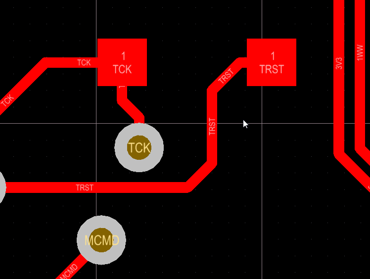
- Enhanced Via Dragging - connected tracks are now adjusted more intelligently, resulting in a neater result (demonstrated in the animated GIF below).
- Automatic Neck-Down - by scoping a routing width rule to target a placement room, the routing automatically adjusts at the room boundary when you interactively route through the room.
- SMD Entry Design Rule - this new rule gives control over how a track and enter or leave an SMD pad (demonstrated in the animated GIF below).
- SMD to Corner Design Rule - this rule is obeyed during interactive routing, working in harmony with the SMD Entry design rule (demonstrated in the animated GIF below).
- Via Under SMD Design Rule - this rule is obeyed during interactive routing, pads targeted by an applicable Via Under SMD design rule can have vias placed in them.
- Routing Layers Design Rule - this rule is obeyed during interactive routing, you can only switch to a signal layer if allowed by the applicable Routing Layers design rule.
Single click and drag to reshape routing
Altium Designer incorporates excellent interactive track manipulation features, which can be used to easily modify existing routing. It now supports direct routing modification, simply click and drag to reshape the routing, the connected segments are automatically updated to maintain the routing quality.

Configure the Dragging options to allow direct dragging, or require selection first.
This change is delivered through new options in the PCB Editor — Interactive Routing page of the Preferences dialog. Under Dragging there are 2 new dropdowns, these are used to configure the default behavior of dragging both a Selected track/via, and an Unselected via/track, to be either a Move or a Drag action. The new default is to Drag when unselected and Move when selected. To mimic the behavior of earlier versions of Altium Designer, set these to Move when unselected, and Drag when selected.
The new default dragging behavior makes it quick and easy to modify the routing - click the image to watch it in action.
Enhanced Via Dragging
In earlier versions of Altium Designer, when a via is dragged the software simply added extra track segments to maintain net connectivity. In Altium Designer 14.3, when a via is dragged the connected tracks are re-routed to suit the new via location, as shown below. In this video the interactive routing mode is set to push.
Via dragging has been improved to give cleaner and more suitable results.
SMD Entry Design Rule
The new SMD Entry design rule ensures that the routing enters and exits the pads exactly where you want it to. The new rule also works in harmony with the SMD to Corner rule, ensuring that the routing exits the pad in the correct location and the first corner is in an appropriate distance from the pad.
To learn more about the new design rule, refer to the SMD Entry rule description.
SMD to Corner Design Rule
In Altium Designer 14.3 the SMD to Corner design rule is not just a post-routing test, it is now obeyed during interactive routing. This simplifies the routing process, ensuring that the first routing corner is a suitable distance from the end of the SMD pad.
The SMD entry and SMD to Corner design rules work together to give cleaner routing results at SMD pads.