PB30 Prototyping Peripheral Board
Contents
Parent article: Peripheral Boards
Altium's Prototyping peripheral board (PB30) provides a rapid prototyping space to quickly test out additional hardware resources – accessible by the User FPGA device on a NanoBoard NB2 or 3000-series NanoBoard. The board offers pre-defined land areas to accommodate SMD components of various pitch, as well as thru-hole components. Through its standard connector, the board provides access to generic IO and services that are common to all Altium peripheral boards.
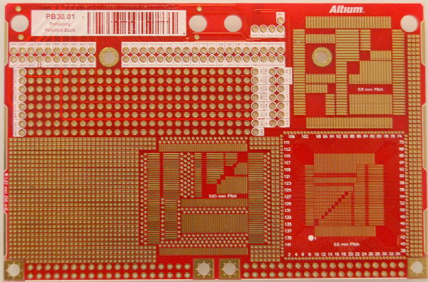
Altium's Prototyping peripheral board PB30 (viewed from the top).
Features at-a-glance
Related article: Peripheral Board Common Services
- Pre-defined land patterns for easy location of surface mount devices with 0.5mm, 0.65mm and 0.8mm pitches. Each SMD pad is connected to a 0.5mm hole to allow simple connections using prototyping wire.
- General purpose area offering 2.54mm (0.1") pitch – perfect for thru-hole components
- General purpose area offering 1.27mm (0.05") pitch – suitable for SMD, with 0.5mm thru-hole located centrally to each SMD pad
- Ability to locate and wire resources on either or both sides of the board – maximizing the prototyping space available
- 1-Wire® memory device used to store board ID and related information
- Single on-board connector follows standard Altium peripheral board pinout providing easy access to the following generic IO and common services:
- 50 x general purpose IO
- Hard and Soft JTAG signals – allowing for inclusion of a JTAG-equipped physical device such as an additional FPGA resource.
- Audio signals – Line In (L+R), Line Out (L+R) and Mic In
- I2C interface – allowing use of resources possessing an I2C-compatible interface.
- SPI Bus interface, with two dedicated chip select lines – allowing for up to two SPI-based resources.
- 1-Wire Bus interface signal – allowing for use of one or more slave 1-Wire compatible devices.
- Four pins made available to receive gated clock signals from the NanoBoard's Host (NanoTalk) Controller (3 clock signals and 1 enable signal).
- Power signals – +5V, +3V3, +2V5, +1V8, +1V2, and GND.
- Standard, double-sized peripheral board
- 3 standard board colors – red, green and blue
- High-quality gold PCB finish
Functional Overview
The following image presents a high-level block diagram of the PB30 Prototyping peripheral board.

Peripheral board PB30 block diagram.
Board Identification
Board identification is handled courtesy of a DS2502 1024-bit, 1-Wire EPROM device (from Maxim).
1-Wire memory used to contain the
ident code for the board.
The DS2502 is primarily used to contain a code with which to identify the peripheral board when plugged in. The Host (NanoTalk) Controller interrogates this device over a single wire, the associated signal of which depends on where the peripheral board is attached:
- Attached to a NanoBoard NB2 –
ONE_WIRE_PB_IDA(if attached to the'PERIPHERAL BOARD A'connector);ONE_WIRE_PB_IDC(if attached to the'PERIPHERAL BOARD C'connector)
- Attached to a 3000-series NanoBoard –
ONE_WIRE_ID
The DS2502 supports half-duplex communication at a rate of up to 16.3kbits/s. Power for the device is sourced over the same single wire as the data itself –- courtesy of a parasitic capacitor which charges when the 1-Wire bus signal line is High.
The DS2502 device (designated U1) is located on the solder side of the board, to the left of the 100-way docking connector. For more information on the device, refer to the datasheet (DS2502.pdf) available at www.maxim-ic.com.
PB30-Specific Resources
The PB30 has no resources in the traditional sense of a peripheral board. Rather it is a blank canvas by which you can attach and wire-up your own resources. Connections to/from generic IO pins, common services and power supplies – delivered through the peripheral board's 100-way connector – can be made quickly using prototyping wire. Simply wire the relevant I/O and control signals from your 'prototyping resource' to the available connection points on the board. These signals are hardwired (via the peripheral board connector on your NanoBoard) to I/O pins of the target User FPGA device – either directly (on a NanoBoard 3000), or indirectly via pins of the relevant daughter board connector (on an NB2).
SMD-Specific Land Areas
The PB30 caters for addition of resources delivered in SMD-based packaging, through provision of several pre-defined land areas. Whether a device you are using has 0.5mm, 0.65mm or 0.8mm pin-pitching, the PB30 has you covered.
Land area catering for 0.5mm pitch SMD components on the top. The bottom side
of the board has a mirrored pattern directly underneath.
Land area catering for 0.65mm pitch SMD components on the top. The bottom side
of the board has a mirrored pattern directly underneath.
Land area catering for 0.8mm pitch SMD components on the top. The
bottom side of the board has a mirrored pattern directly underneath.
Using a 1.27mm pitch SMD component? No problem. Simply locate it on the 1.27mm pitch general purpose prototyping area (see next section).
Each SMD pad is routed to a 0.5mm plated thru-hole, allowing you to connect to another area of the board, or directly to one of the predefined signal connection points, as you wish using prototyping wire.
General Purpose Land Areas
The PB30 provides general purpose prototyping areas in 1.27mm (0.05") and 2.54mm (0.1") pitches. The main 0.1" area can be found directly next to the signal connection points, with further areas offering this pitch located at the bottom edge of the board. These areas are particularly suited to thru-hole components.
Main general purpose prototyping area with 2.54mm (0.1") pitch, as seen from the top of the board.
The main 0.05" area can be found directly beneath the main 0.1" area, and encapsulates the 0.65mm pitch area for surface mount devices. A further general purpose area with this pitch is located along the right hand edge of the board (looking from the top side). These areas can accommodate surface mount devices (for example, 0406 resistors sit nicely here!), as well as 0.1" pitch components. They also provide a quick through-board connection.
Main general purpose prototyping area with 1.27mm (0.05") pitch, as seen from the top of the board. Note
that the 0.65mm pitch SMD land area resides within the bounds of this general purpose prototyping area.
Signal Connection Points
The predefined signal connection points provide the interface between your prototyping resources and the generic peripheral board signals channeled through the board's 100-way connector. Connection points are available (and clearly labeled) for each of the general I/O, common service and power supply signals.
Signal connection points - your interface to the target User FPGA, as well as common services and power
supplies from the recipient NanoBoard.
The following table lists the various generic signals that are common to all Altium peripheral boards, and how they are labeled on the PB30.
| Signal Description | Signal Naming on Schematic | Connection Point Labeling on PB30 |
|---|---|---|
| 50 general purpose I/O signals |
|
|
| Hard JTAG signals |
|
|
| Soft JTAG signals |
|
|
| Audio signals |
|
|
| I2C interface signals |
|
|
| SPI interface signals |
|
|
| 1-Wire interface signal |
|
|
| Gated clock signals |
|
|
| Power supplies |
|
|
Your prototyping resources might include JTAG-equipped physical devices (e.g. an FPGA) featuring designs that include Nexus-enabled (Soft) devices. The NanoTalk Controller on the NanoBoard – into which you plug your PB30 peripheral board – will only route the Hard and Soft JTAG chains via the peripheral board connector if the signal level on pin 23 of the connector (signal JTAG_CNCT on the peripheral board) is Low. Within the signal connection points, you will find this signal labeled JTAG EN.
Design Interface Component
The following table summarizes the available design interface components that can be placed from the FPGA PB30 Port-Plugin.IntLib, to access the 50 general purpose IO lines for the PB30, when attached to a NanoBoard 3000 or NanoBoard NB2.
|
Component Symbol
|
Component Name
|
Description
|
|---|---|---|
|
| NANOCON50IOB | Place this component to access the 50 general purpose IO lines of the attached PB30 in bussed format. The port is bidirectional, allowing use of any line as input or output. |
|
| NANOCON50IOS | Place this component to access the 50 general purpose IO lines of the attached PB30 in single pin format. Each individual port is bidirectional, allowing use of the corresponding line as either input or output. |
|
| NANOCON25I25OB | Place this component to access the 50 general purpose IO lines of the attached PB30 in bussed format. Two dedicated ports are provided, splitting use of the lines into 25 inputs and 25 outputs respectively. |
|
| NANOCON25I25OS | Place this component to access the 50 general purpose IO lines of the attached PB30 in single pin format. Dedicated input and output ports split use of the lines into 25 individual inputs and 25 individual outputs respectively. |
|
| NANOCON17I17O16IOB | Place this component to access the 50 general purpose IO lines of the attached PB30 in bussed format. Three dedicated ports are provided, splitting use of the lines into 17 inputs, 17 outputs and 16 bi-directional lines respectively. |
|
| NANOCON17I17O16IOS | Place this component to access the 50 general purpose IO lines of the attached PB30 in single pin format. Dedicated input, output and bi-directional ports split use of the lines into 17 individual inputs, 17 individual outputs, and 16 bi-directional lines respectively. |