A Suggested Methodology for Vault-Driven Electronics Design
Contents
- Setting up Version Control
- Components Folder Structure
- Design Content Folder Structure
- Hardware Design Folder Structure
- Using Templates to Speed Design Project Creation
- Linked Output Job Configuration Files
- Keeping Panels and Designs Separate
- Setting up an Altium Vault
- Vault Structure
- Vault Item IDs
- Revision Naming and Lifecycle Management Schemes
- Managing Vault Users and Permissions
- If it's not in a Vault - Create and Release!
- Models
- Schematic Symbol
- PCB 2D/3D Component Model
- Generic Models
- Components
- Sourcing Component Models
- Managed Sheets
- Naming Convention
- Design Standards
- Configuring and Releasing Designs
- Using Standard Configurations
- The Release Process
- Controlling Data Access
Parent article: Vault-Driven Electronics Design
Using its own unified electronic product development software – Altium Designer – in concert with its suite of advanced design data management features and Vault Technology, Altium continues to forge a new, streamlined methodology for designing electronics. This methodology – essentially optimizing the design flow by using the tools and technologies in the manner in which they were designed to be used – is centered around the concept of designing for reuse, and that all elements of design (models, components, schematic sheets, design modules, etc) have been released into, and therefore can be sourced from, an Altium Vault. As such, this evolving methodology is known as Vault-Driven Electronics Design.
The benefits of adopting this design methodology include the enhanced quality of the designs created, since all design elements are managed in the vault and ratified for use, and the inherent high-productivity gains of being able to quickly create designs using an ever-expanding repository of design 'building blocks'.
In this article, we will take a look at the Vault-Driven Electronics Design methodology, as it is currently defined and implemented by the Hardware Team at Altium today. Tutorial-like, but not rigidly so, think of this article as more of a conversational 'walk through' of the methodology –- providing an overview of its key elements and how various aspects of Altium Designer and Altium Vault Technology are being used to streamline design.
Setting up Version Control
Related article: Securing Design Source Inside a Design Repository
Version control and Altium Vault Technology are essentially symbiotic partners in the design ‘dance’. While Vaults offer a secure repository for the released data, and are the source from which all elements in a new design project are placed, it is a version control repository – known within Altium's Design Data Management system as a version-controlled Design Repository – that stores the design-side source itself, the source that gets incrementally changed by a design team on a day-by-day basis, and released (and re-released) into a vault as a series of evolutionary revisions of linked design items.
So the source design project lives and breathes within a version control repository. The electronics - the features and functionality - are implemented in the design using vault-based components, managed sheets, and higher level assemblies (such as module boards), the design-side source for which is also stored within the version control repository. Changes are made by any member of the design team and recorded the instant they check in a change to the SVN or CVS repository. At all times the process is fully auditable - who changed what, in which document, and when. The design project, at the appropriate stage, will then be released into the vault itself, along with the generation of all applicable data required to fabricate and assemble that board downstream.
The Altium design methodology also relies heavily on version control as the dwelling place of design templates and to implement the concept of common files that are shared by design projects. So a structure of project template files and applicable linked source documents. The designer comes to the version control repository to checkout these files locally, and use the project templates as a means to get the ball rolling for any new design project that comes along.
Altium Designer supports version-controlled Design Repositories using either Subversion (SVN) or Concurrent Versions System (CVS) as the service provider. Subversion is the preferred provider and Altium Designer, true to its unified nature, comes with Subversion capabilities built-in. To quickly create a new folder-based SVN Design Repository:
- Open the Preferences dialog
- On the Data Management – Version Control page, you will see that
SVN - Subversionis an enabled version control provider, and that the built-in Subversion is enabled for use by default. - On the Data Management – Design Repositories page, click the Create New button and choose the SVN entry on the associated drop-down menu. Use the Create SVN Design Repository dialog that appears to give the vault a meaningful name, specify a default checkout path, and specify the location for the repository. If a folder is specified that does not currently exist, it will be created for you.
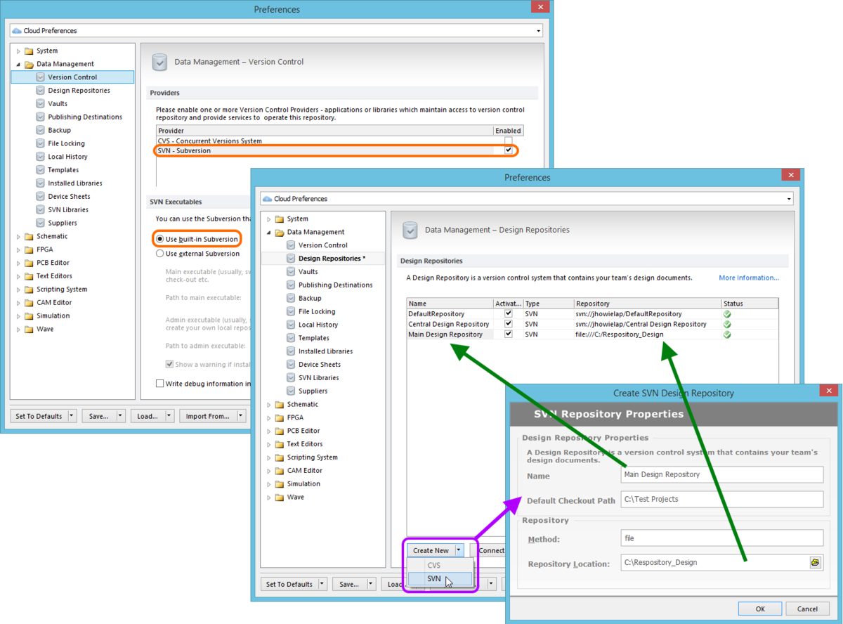
Example newly created SVN Design Repository, appearing within Altium Designer as Main Design Repository.
To have even better separation and easier-implemented control over just who has access to which area of design, it is recommended to set up three distinct folders within the repository:
- One for Components.
- One for Design Content (managed sheets).
- One for the actual Hardware Designs (including any modular design building blocks, production designs, and manufacturing panels).
Then use folder-level permissions to determine who has access to which area.
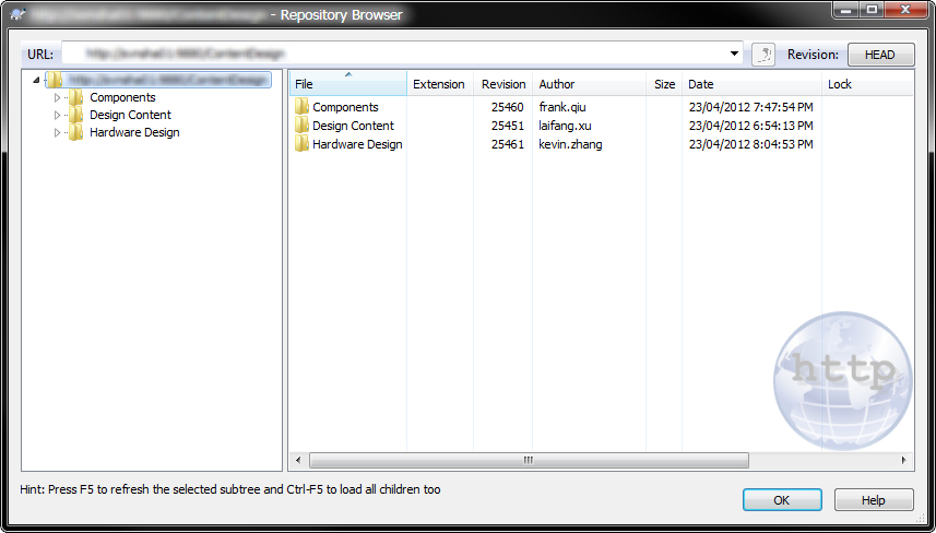
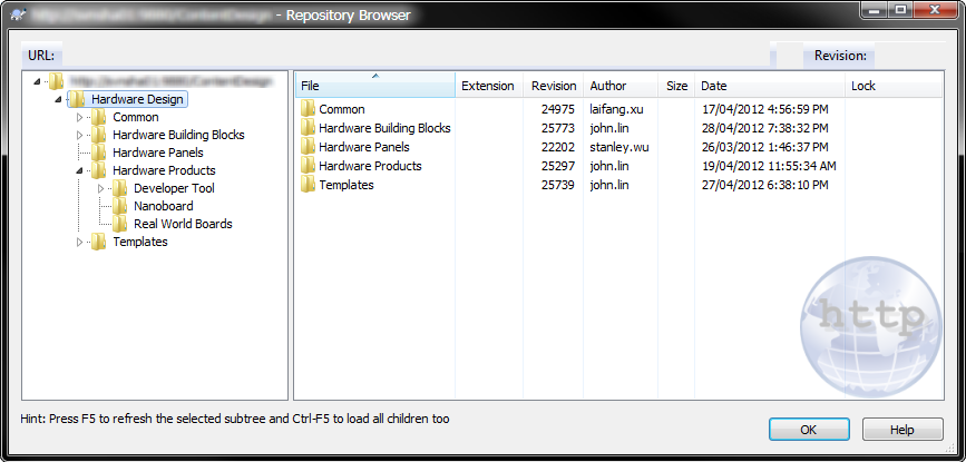
Browsing an example SVN version control repository containing separate folders for each of the three areas.
The following sections take a closer look at the structure in-place for each of these folders, including certain source design documents that play a vital role in the design methodology. Getting the structure implemented correctly is paramount, since this structure will ultimately be reflected, or at least a large part of it, in the target vault, creating a 1-to-1 relationship by which the designer can easily browse and locate between design-side source and released managed Items in the vault.
Components Folder Structure
Component folder structure in the SVN repository.
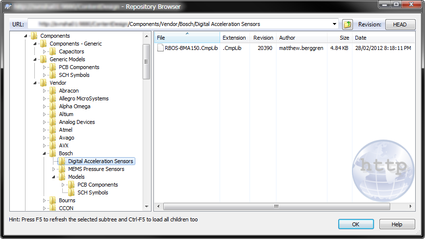
The Components folder contains three sub-folders:
- Components - Generic: components that can be highly parameterized, such as resistors, capacitors and inductors. Each component type is further categorized as necessary, depending on its parametric nature. So in the image below, Capacitors are further divided by material, then size, then voltage. Notice that there is no
Modelsfolder. Since these components are generic, they make use of generic schematic symbol and PCB 2D/3D component models.

- Generic Models: these are models that can be reused across vendors and also for generic components (where multiple components change in some parametric way rather than in their domain model representation). For almost all vendor components, the PCB 2D/3D models are specific and will therefore be local to those components. There will therefore be very few of these. It is more the schematic symbols that come into play here.
- Vendor: components from a third party manufacturer, organized by vendor and further categorized by family. So in the example image below, there is a folder for the vendor
Bosch, and then sub-folders for the familiesDigital Acceleration SensorsandMEMS Pressure Sensors. These family names are generally taken directly from the vendor's website. A separate folder is used to store the specific models for these components – further sub-divided into folders for the schematic symbols and PCB 2D/3D component models.
Design Content Folder Structure
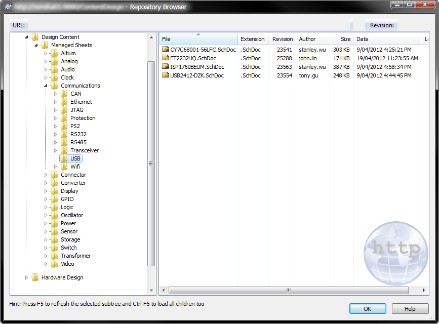
Design Content folder structure in the SVN repository.
The Design Content folder contains a sub-folder of schematics that are the source for Managed Sheet Items in the vault. A Managed Sheet is an Altium Designer schematic sheet containing components (sourced from a vault) and wiring, that is then released to an Altium Vault, so it can be re-used in other designs. The Managed Sheet concept is not limited to a single schematic sheet either, you can place a Managed Sheet in your design that is the top of a tree of other Managed Sheets.
These source schematics are structured by functional class and sub-class (where appropriate). At the component-level, grouping together by vendor and component families makes sense, but at this managed sheet level, where a sheet can contain components from different vendors, it's more appropriate to talk about what the sheet contains, or rather the functionality that it offers the designer. In the vault especially, this will enable a designer to quickly flick through and browse to the sheet required, based on the functionality it offers.
This ability to use components to build larger design building blocks enables the design-flow to become streamlined. The designer, just like picking parts off a shelf, simply reuses these managed sheets of design functionality in the bigger design project.
Hardware Design Folder Structure
Hardware Design folder structure in the SVN repository.
The Hardware Design folder essentially contains the following five sub-folders:
- Common – this folder contains documents that are common to design or panel projects. There is a folder of pre-configured Output Job Configuration files, that are used in all design projects. There is also a folder of PCB panel documents, which are used in panel projects.
- Hardware Building Blocks – this folder is used as the location for design projects which themselves will become modular design elements that can be reused in other 'parent' designs. Altium's Hardware Team for example, design module boards. These boards can go for manufacture themselves in their own right, but are also used as satellite boards that attach to parent 'carrier' boards. When it comes time to manufacture and assemble the parent board, a module board is picked and placed as though it were a component.
- Hardware Panels – this folder is used as the location for panel projects, keeping panels distinctly separate from the boards they will ultimately contain for fabrication.
- Hardware Products – this folder is used as the location for full product designs that will be used as products in their own right out in the real world.
- Templates – this folder contains template project and document files used to streamline the start of new designs.
Using Templates to Speed Design Project Creation
An important part of Altium’s design methodology is the ability for a designer to get going on a new design quickly, and in a streamlined way. To support this, the idea of using templates and common files naturally evolved. This involves templating as much of the design-side source as possible, giving a designer all the bits and pieces they need to get started with that next big design. For Altium's Hardware Team, developing module boards, this meant creating a range of PCB project templates to cater for different board form factors and layers, with links to the relevant schematic and PCB document templates.
All of these template files are created and stored in their respective locations under the \Hardware Design\Templates folder. So to run through how the Hardware Team are using templates, let's first look at the structure beneath the Templates folder.
Templates folder structure, as implemented by Altium's Hardware Team.
Templates are divided into Projects, and their constituent Documents. There are both board-level and panel-level project templates (more on why these are separated later). The Team currently have project templates defined for the module boards they are working on, and these are parked under the aptly-named Projects\Board Level\Building Blocks sub-folder. Likewise, related panel project templates are stored under the Projects\Panel Level\Building Blocks sub-folder. In terms of board-level project templates, there are separate folders for each of the various board dimension/layer configuration combinations. For the panel projects, there is a folder for each panel dimension/layer configuration combination.
Project templates in the SVN repository.
Now, running with a board-level project template, this references, or links to, required schematic and PCB document templates. These are stored in the Documents\SCH Documents and Documents\PCB Documents folders respectively. Links from the main project file to any constituent documents are always kept relative. The following image shows the schematic document templates used by the Hardware Team.
An example of defined Schematic document templates (as used by the Hardware Team).
Two template documents (*.SchDot) have been defined – for A3 and A4 sheet sizes respectively – from which a set of top-level schematic document templates have then been created, for use across the range of Altium's module board designs. Each document is named to indicate which of the standard Altium module sizes it can be used for. For example the document MBxxxx_Top_P016-M9X9_A4.SchDoc is the top-level sheet containing the necessary vault-managed component for a 16-pad, 9x9mm module. As such, it would be the sheet used (linked into) any of the three template projects for this module board size.
A blank, generic devices template document has also been created (MBxxxx_Devices.SchDoc), which serves two uses – as the head document in a hierarchy of managed sheets in a module design project, and as the blank canvas for building a functional sub-circuit, to be released and reused as a managed sheet.
The following image shows the PCB document templates used by the Hardware Team. Notice that the PCB document naming is identical to that of the project itself, making it easy for a designer to verify they have the right document in the right project.
An example of defined PCB document templates (as used by the Hardware Team).
The result of using this template-driven approach is that the designer can simply browse through project templates, choose the one that matches the requirements of their next design project and open a new project in Altium Designer with all base-level design documents brought-in. They are no longer distracted with having to set up these documents, they are right there from the start.

Start a new design and have all the right documents in place, ready to go, simply by clicking on a board project template.
Notice in the image above that Output Job Configuration files are also linked and brought in to the project. These are not defined as template files, but rather as a set of common files, as discussed in the next section...
Linked Output Job Configuration Files
Further streamlining the design flow, a set of pre-configured Output Job Configuration files are available for use by design projects - defined so that the correct output files are generated each and every time across all designs that use them, without the designer having to touch or modify them in any way. The standard set includes separate files for Fabrication, Assembly and Documentation outputs, as well as a file to cover Validation reports. This latter file is used only for board-level designs, and is used by the Validation stage of the board release process. To cater for board designs with different layer configurations, specific Fabrication Output Job files are used – so one specific to a 2-layer board, one for a 4-layer board and one for a 6-layer board. So a set of Output Job files to cover the needs of all potential design projects.
In the SVN folder structure, these files are stored in the \Hardware Design\Common\Output Jobs folder.
An example of defined common Output Job files (as used by the Hardware Team).
Each of the template projects simply links-in the required set of files from this common folder.
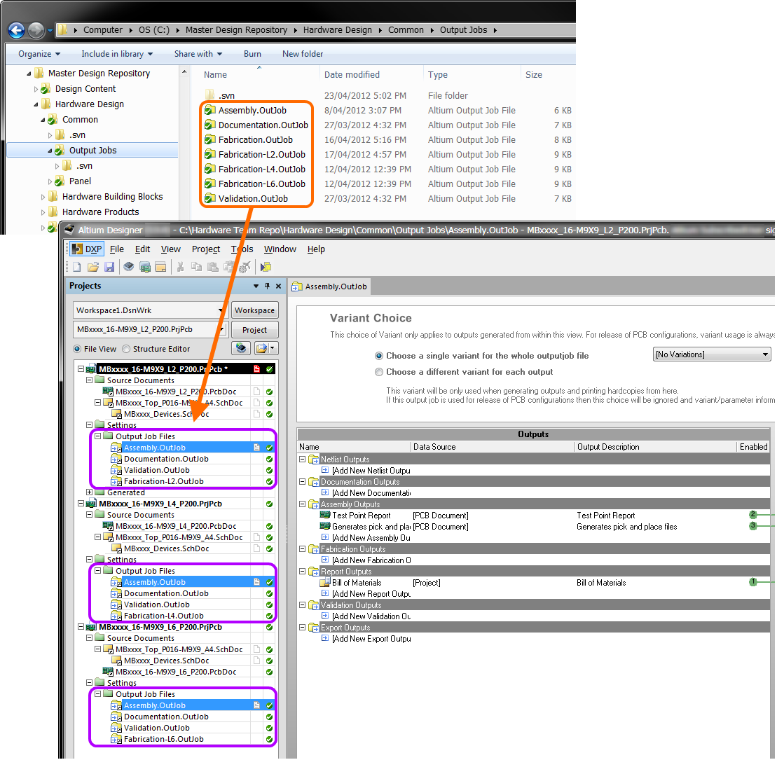
The relevant common Output Job files are linked to the project templates. When a designer clicks to use a project, the Output Job files are brought into the project - one less worry for the designer!
As an indication of the outputs defined within each of the specific OutJobs, the Hardware Team use the following:
Fabrication.OutJob/Fabrication-L2.OutJob/Fabrication-L4.OutJob/Fabrication-L6.OutJob– ODB++ Files, Gerber Files, NC Drill Files.Assembly.OutJob– Test Point Report, Pick and Place Files, Bill of Materials.Documentation.OutJob– PCB 3D Print, Schematic Prints, Bill of Materials.Validation.OutJob– Design Rules Check, Electrical Rules Check.
A designer shouldn't need to change these files. They are configured to produce the right manufacturing information from the start. But, should a file need to be modified in any way, its storage within the SVN Design Repository comes into play. Since the board release process – releasing a configuration of a board design to a new revision of a linked Item in a target vault – checks out and works with the HEAD revision of the source project from the Design Repository, a file must be checked back in for any change to 'take effect'. The instant a file is checked in, it is stamped with who modified it, and when. So there is full accountability, and no circumventing the system!
Keeping Panels and Designs Separate
Another aspect of the design methodology is that panel files are not stored as part of the board-level design projects. Rather separate panel projects are used. The reason being that a panel is rarely ever used to fabricate a single board – and one panel may be used to fabricate a number of different boards. So a panel is conceptually very different to a standard board-level design, in terms of what is ultimately being manufactured, and is therefore released to the vault as a distinct Item in its own right.
So, as we saw previously, there are template projects in place for each of the panel dimension/layer configuration combinations. Each project references an identically-named PCB document, which is stored as part of a set of common panel PCB documents, in the \Hardware Design\Common\Panel folder. The project also references the relevant Output Job files, from the common set. The exception is the Validation.OutJob file. This is not required, since it is assumed that all validation is performed at the board design level, and so everything should be valid by the panelization stage.
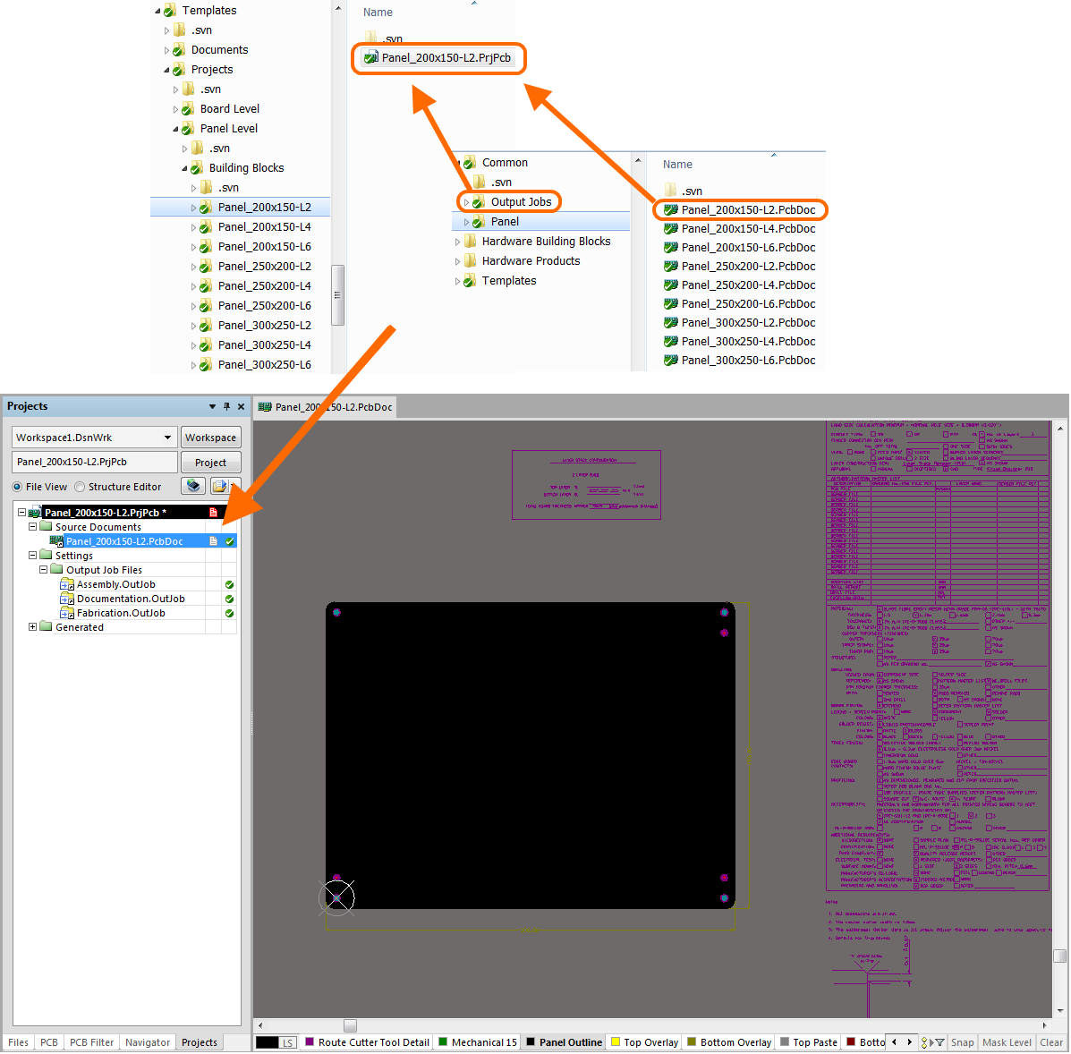
Start a new panel and have all the right documents in place, ready to go, simply by clicking on a panel project template.
Setting up an Altium Vault
Related article: Altium Vault
The Altium Vault plays a fundamental role in Altium’s design methodology, as coined by the catchphrase ‘Vault-driven Electronics Design’. The vault is THE destination for all elements of design. It provides a single location that designers company-wide can go to, to source the required building blocks for their next design projects. Or, from another perspective, the vault is a single repository for storing the collective design intelligence of an organization’s engineering community. At any time, a designer in that organization can come to leverage existing design items for reuse in their own designs, ‘off-the-shelf’ as it were.
Altium’s Vault Technology provides the security and data management features to ensure that designers can be confident in the integrity and state of any item in the vault that they wish to use in their designs. The integrity comes through the process of releasing the design-side source data into the vault as a locked-down, non-editable revision of that particular item. Lifecycle management reflects what the item can then be safely used for, for example prototyping, production, and so on. In other words, the designers work only with design items that have been approved for use in designs by company management. They simply need to come into the vault and ‘cherry pick’ the bits and pieces they need to speed the creation of a new design.
And the term ‘vault-driven’ really reflects a key aspect of the design methodology, and that is that ONLY items from a vault can be used in a design. So first look in the vault for existing components, managed sheets of specific circuit functionality and any higher-level design assemblies. If a design element does not exist in the vault, create it and release it as a new design item into the vault first, before reusing it in a design.
Accessing your Altium Vault from within Altium Designer is a case of connecting to the vault, and also signing into the vault platform - giving access to other services delivered through the vault's installation, in addition to the vault service itself. Connecting and signing in to the Altium Vault can be done in the following ways:
- Use the Sign in Altium Vault command from the DXP menu.
- Add a connection to the vault from the Data Management - Vaults page of the Preferences dialog.
- Click the Sign in Altium Vault control, on the System — Altium Vault page of the Preferences dialog.
Irrespective of method used, the connected vault will be apparent in the Vaults listing, on the Data Management - Vaults page of the Preferences dialog.
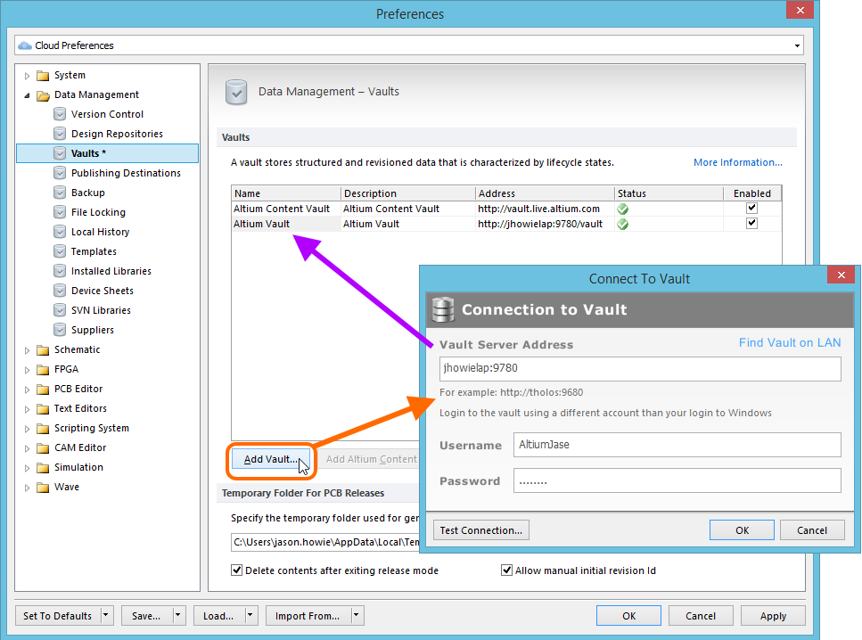
Example of a connected Altium Vault, appearing within Altium Designer as Altium Vault.
You can also connect to Altium's own vault - the Altium Content Vault - and the wealth of design content it offers. This vault houses all data under the following top-level folders:
Board Templates– offering board templates, managed sheets, and board connector components.Unified Components– offering vendor-specific families of components, as well as generic components including capacitors and resistors.
To connect to the vault, simply access the Data Management – Vaults page of the Preferences dialog, and click the Add Altium Content Vault button. Provided you have a licensed instance of Altium Designer and valid Altium Subscription, a connection to the vault will be made instantly. This direct connection enables you to access and place content from the Altium Content Vault directly into your designs, through the Vaults panel.
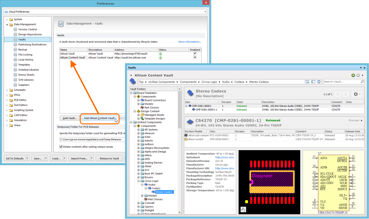
Access and connect to Altium's own vault - the Altium Content Vault - and the considerable design content it contains.
Vault Structure
A sense of logical order is brought to a vault by creating a tree of folders for the various Items stored in that vault. This is primarily performed from within the Vaults panel. A number of folder types are available, use these to categorize the vault content. Best practice is to have a 1-to-1 match between the structure in the SVN Design Repository and that in the Altium Vault. This keeps a direct (and clean) relationship between source in VCS and the corresponding linked managed items in the vault, making it easy for anyone in the design team to move between the two and find what they need.
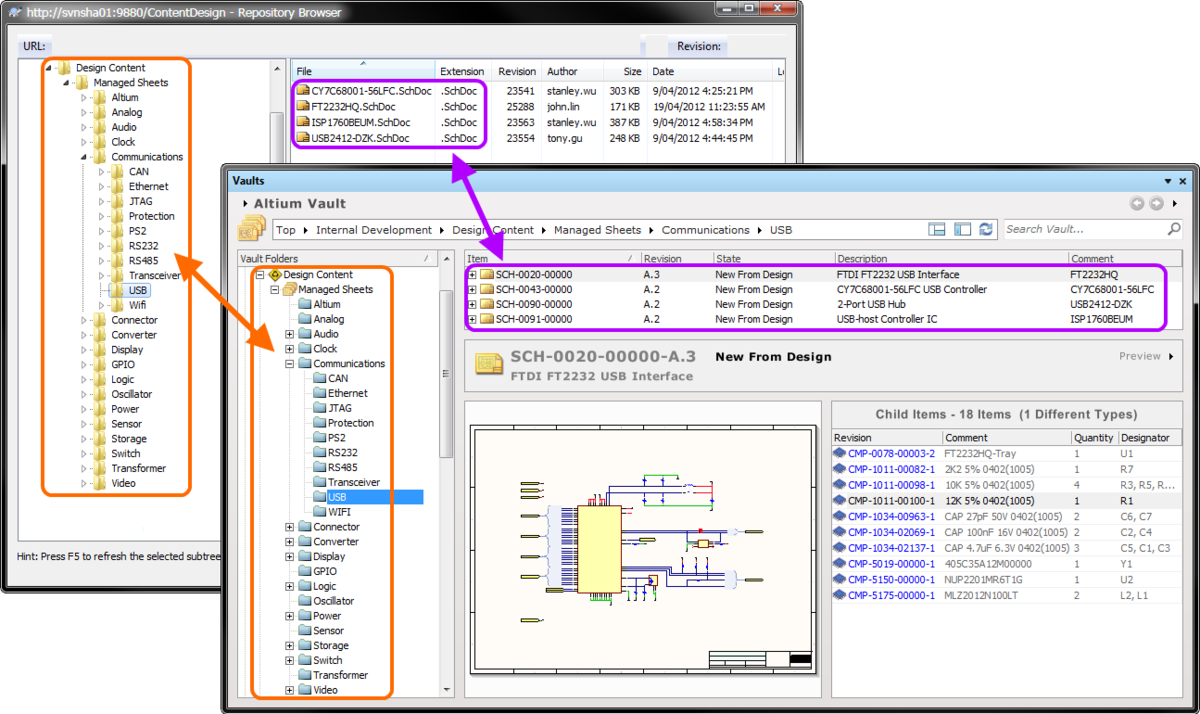
The same storage structure is used in the Altium Vault and the SVN Design Repository, making it easy for a designer to find what they need on both sides of the link.
Vault Item IDs
Each distinct design-side source element (models, components, schematic sheets, project configurations) is released to the vault as revisions of a linked item. Each item has its own unique Item ID. The design methodology includes the following scheme for how these IDs should be named.
Revision Naming and Lifecycle Management Schemes
Related articles: Item Revision Naming Schemes, Item Lifecycle Management
Altium's design methodology uses the following Item Revision Naming schemes and Lifecycle Definitions for the various design items that can be released to a vault.
| Design Item | Revision Naming Scheme | Lifecycle Definition |
|---|---|---|
| Models | 1-Level (e.g. 1) | Basic Lifecycle |
| Components | 1-Level (e.g. 1) | Component Lifecycle |
| Managed Sheets | 2-Level (e.g. A.1) | Component Lifecycle |
| Design Projects | 3-Level (e.g. 01.A.1) | Structured Lifecycle With Approvals |
Observing standard revision naming schemes and lifecycle definitions, across the various types of design item in a vault ensures smooth, consistent management of those items. So at the lowest level, models use 1-level revision naming with basic lifecycle management (they’re either ready for design reuse or not!). Components and managed sheets use the same component lifecycle management, but differ in their revision naming schemes, using 1- and 2-level schemes respectively. For a model or component, any change is going to be significant, but for a managed sheet, a 2-level scheme suits minor revisions (text changes for example) and major revisions - something that changes the circuit or functionality of that circuit substantially.
Managing Vault Users and Permissions
Related article: Controlling Access to Vault Content
An Altium Vault provides secure handling of data with high integrity, while providing both Design Team and Supply Chain access to that data as needed. This latter aspect, of who can access a vault, and more importantly what data they are allowed to access, is facilitated by the Altium Vault's user access control and sharing capabilities. These can be broken down into the following key areas:
- User Management – which people are able to connect to the Altium Vault (through Altium Designer or an external browser). Management of users, as well as defined Roles (groupings of users), is performed using the vault's browser-based interface. This can be done either from an external browser or via the relevant views under Altium Designer's Home page. For detailed information, see Browser-based Access and Management of an Altium Vault.
- Folder-level Sharing – providing the ability to control who is able to see what content in the vault by sharing vault folders. This allows control over whether other users can simply view a folder and its content, or also edit it (effectively releasing design data into it). A single vault can be partitioned into various effective 'zones' of content, but with controlled folder-level permissions, the content can be made selectively visible, or hidden, as required, giving the right people, the right access, to the right data.
- Item-level Sharing – providing the ability to control who is able to see which Items in a shared folder. Think of this as a finer level of sharing, in contrast to the coarser level of sharing provided through folder access control. Provided a user has access to the folder itself, they will then be able to view/edit (as permitted) Items within that folder that are shared with them.
- Item Revision-level Sharing – providing the ability to control who is able to see which revisions of a shared Item. Think of this as the finest level of sharing. Provided a user has access to a parent Item itself, they will then be able to view/edit (as permitted) revisions of that Item that are shared with them.
- Revision Data Access Control – providing the ability to manage access to an Item Revision's data for a released PCB design, allowing users to see only the portion of data they are allowed to see, while by-passing the need for additional publishing.
If it's not in a Vault - Create and Release!
The very essence of vault-driven design is that every design element used in a design must be sourced from an Altium Vault. Plain and simple – if a component, managed sheet or full design module sub-assembly is required to be used in a design, and that item is not currently found in any connected vault, then said item must be built/created and released into the vault. This paves the way to another equally important concept of the vault-driven design methodology, and that is the philosophy of designing for reuse. So creating and releasing design elements into a vault that will, in turn, be available for use again as source design items in future designs.
And by adopting the mantra of 'designing for reuse', your engineering team will not only nurture and grow an impressive repository of reusable design elements, but also benefit from the ability to build future designs expediently through their availability. And safe in the knowledge that all of these design reusables are securely managed, audited and ratified for use.
In fact, Altium's Hardware Team never kick-off a new design without first scoping everything that is needed in that design. So what circuits are required, what components. They then trawl their Altium Vault to see which of those design elements already exist and can be quickly reused in their new designs. And if they find something is not there, they build and release it so that it IS there. All this work is performed prior to selecting a project template and entering the 'design arena'.
The following sections take a look at aspects of the design methodology in relation to the design-side source when building and releasing models, components and managed sheets. The actual mechanics of releasing are not covered here, but can be found in the indicated related articles for each section.
Models
Related article: Vault-Based Domain Models
Before you can delve into the process of defining design components and releasing them to a vault, you must first ensure that all the models themselves – representing those components across the various required design domains – have been created and released to the vault. For board-level components this will generally be a case of schematic symbol and PCB 2D/3D component models.
Schematic Symbol
A drawn schematic symbol within a Schematic Library document (*.SchLib) on the design side is mapped to a Schematic Symbol Item in an Altium Vault. Each release of the library stores the symbol model data into a new revision of that Item.
In terms of naming, each Schematic Library file is named according to the following format:
<Vendor Code>-<Part Name>-<Package Name>
where,
Vendor Codeis a unique identifier that is used to associate the model file with a specific vendor (e.g.RBOSfor Bosch,HONfor Honeywell,MCHPfor Microchip, and so on).Part Nameis a short name that uniquely identifies the part that the symbol represents. This is typically the vendor's specific order code for the part, without the packaging info (e.g.BMP085for the BMP05 Digital Barometric Pressure Sensor, from Bosch;HMC5843for the HMC5843 3-axis Digital Compass, from Honeywell;MCP4141for the MCP4141 7/8-bit Single SPI Digital POT, from Microchip).Package Nameis the package name for the associated footprint, since the same symbol could be used for a component, in association with a range of different package styles. This name is taken directly from the package specifications that the vendor puts up on their website through data sheets, package documents, or the like (e.g.LCC-8(from Bosch),LPCC-20(from Honeywell),DFN8(from Microchip)).
So full example file names based on this scheme are:
RBOS-BMP085-LCC-8.SchLibHON-HMC5843-LPCC-20.SchLibMCHP-MCP4141-DFN8.SchLib
Delivering consistency, the actual symbol within a file uses the exact same name as that file.
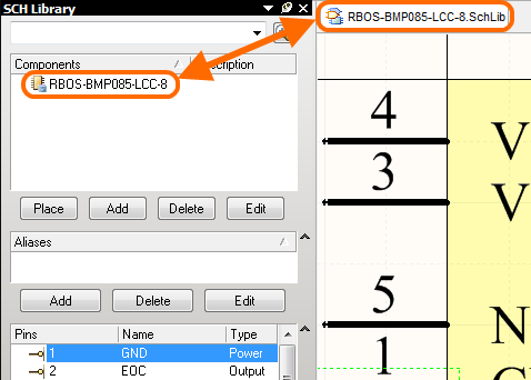
The same naming is used for the file and the symbol within that file.
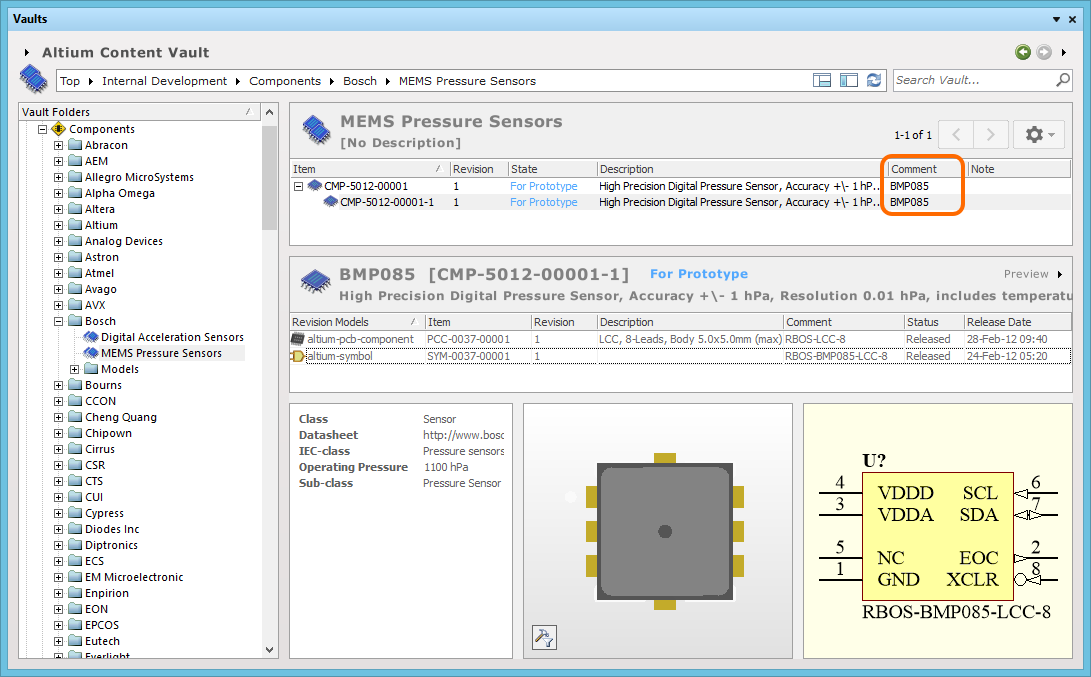
When released into a vault, the name of the source symbol appears as the Schematic Symbol Item's Comment. Coupled with using the same storage structure in both Design Repository and Altium Vault, a designer can quickly browse between the two and find either the design-side source or released design item. And having the symbol name appear as an Item's comment enables quick identification of which symbol is which, without having to remember any Item IDs!
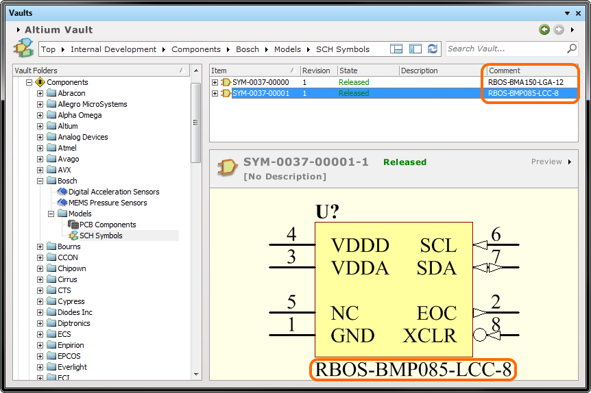
The source symbol name is reflected in the Schematic Symbol Item's Comment field.
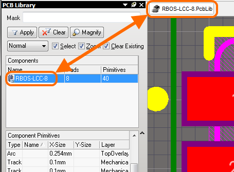
PCB 2D/3D Component Model
A PCB 2D/3D component model within a PCB Library document (*.PcbLib) on the design side is mapped to a PCB Component Item in an Altium Vault. Each release of the library stores the model data into a new revision of that Item.
In terms of naming, each PCB Library file is named according to the following format:
<Vendor Code>-<Package Name>
where,
Vendor Codeis a unique identifier that is used to associate the model file with a specific vendor (e.g.RBOSfor Bosch,HONfor Honeywell,MCHPfor Microchip, and so on).Package Nameis the package name for the footprint, taken directly from the package specifications that the vendor puts up on their website through data sheets, package documents, or the like (e.g.LCC-8(from Bosch),LPCC-20(from Honeywell),DFN8(from Microchip)).
So full example file names based on this scheme are:
RBOS-LCC-8.PcbLibHON-LPCC-20.PcbLibMCHP-DFN8.PcbLib
Delivering consistency, the actual model within a file uses the exact same name as that file.
The same naming is used for the file and the model within that file.
When released into a vault, the name of the source model appears as the PCB Component Item's Comment. Coupled with using the same storage structure in both Design Repository and Altium Vault, a designer can quickly browse between the two and find either the design-side source or released design item. And having the model name appear as an Item's comment enables quick identification of which model is which, without having to remember any Item IDs!
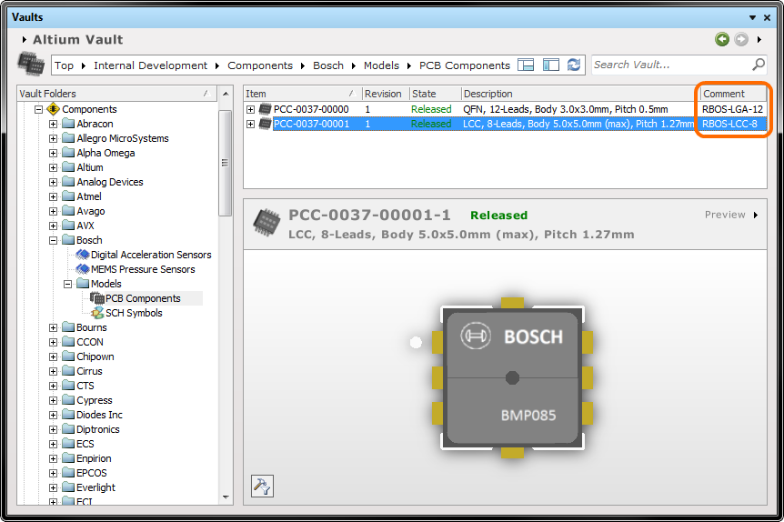
The source model name is reflected in the PCB Component Item's Comment field.
Generic Models
When creating generic models, for use by components across vendors, the naming scheme used is slightly different. And we are talking here about schematic symbols, since footprints are rarely generic. So when creating a generic schematic symbol, the Schematic Library file (and also symbol therein!) is typically named according to the following format:
<Symbol Type>_<Pin Naming>-<Pin Count>
where,
Symbol Typeis an identifier to the functionality or type of component that is being represented by the symbol.Pin Namingis the encoded pin assignment (the functionality of each pin of the device).Pin Countis, as its name suggests, the number of pins the component, which this symbol represents, possesses.
So example filenames are:
NPN_B1E2C3-3.SchLib– containing the symbol for a 3-pin NPN transistor, with Base=pin1, Emitter=pin 2 and Collector=pin 3.DSKY_K1A2-2.SchLib– containing the symbol for a 2-pin Schottky Diode, with cathode=pin1 and anode=pin2.LED_RGB_K1A2K3K4-4.SchLib– containing the symbol for a 4-pin RGB LED, with cathode1=pin1, common anode=pin2, cathode2=pin3 and cathode3=pin4.
Since the symbol name is reflected in a Schematic Symbol Item's comment field, when released into a vault, having this pin assignment encoded means that a designer can browse through the symbols available in the vault and readily identify which one they need to link-in to a component they are creating. The designer has all the information they need to know exactly how the symbol is used, without having pin assignments explicitly drawn as part of the symbol.
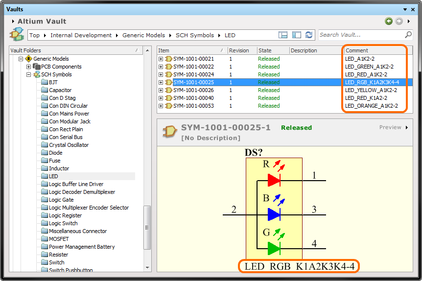
Inheriting the symbol name, symbol items in a vault can be browsed quickly by their comment field, with the encoded pin information quickly revealing how a particular component is configured.
Components
Related articles: Vault-Based Components, Releasing a Component Definition to a Vault
In accordance with the design methodology, any component used in a design must be sourced from a vault. So if a component you need does not currently exist in a vault, it needs to be defined and released. Under no circumstances should a non-vault component be used in design. On the design-side, this means creating a Component Definition.
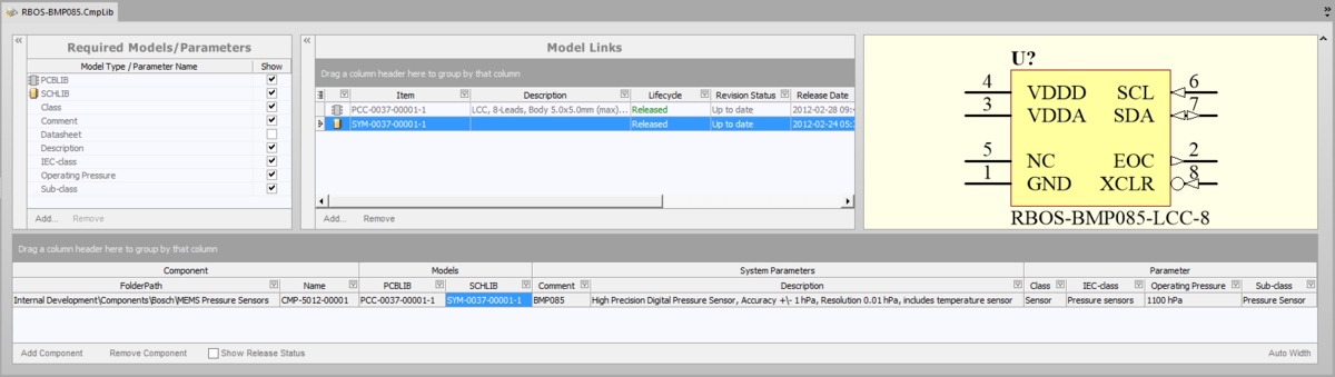
A component definition is simply just that – a definition of a particular design component. A definition that ties together the required models and parameters for that component in a clean and ordered fashion. Each component definition on the design-side maps to an Item – a Component Item – in a target Altium Vault. To put this another way, you are defining the source definitions that will, when released, provide a set of components which you can re-use again and again in your designs.
A component definition is created and managed within a dedicated Component Library file (*.CmpLib), and the design methodology adheres to the use of one component definition per Component Library file.
Example component definition.
In terms of naming, each Component Library file is named according to the following format:
<Vendor Code>-<Complete Part Order Code>
where,
Vendor Codeis a unique identifier that is used to associate the component with a specific vendor (e.g.RBOSfor Bosch,HONfor Honeywell,MCHPfor Microchip, and so on).Complete Part Order Codeis the full name of the item when ordering it from a vendor.
So full example file names based on this scheme are:
RBOS-BMP085.CmpLibHON-HMC5843-TR.CmpLibMCHP-MCP4141-502EMF.CmpLib
Define the component as required, linking-in the required models, defining parameters and entering their values, and so on. With respect to the definition itself, there are some key aspects of the design methodology to observe here:
- The entries for Lifecycle Definition and Revision Naming, in the Document Options dialog (Edit » Document Options), are set in accordance with the schemes employed for this type of design element –
Component Lifecycleand1-Level Revision Schemerespectively. - The models required to represent the component in its various design domains need to exist already in a vault. If not, they need to be! Remember the spiral nature of designing for reuse – where each subsequent design element must be created and released into the vault, ready to be used in the next higher-level design element. The source vault is typically the same, but may be different, especially if using models sourced from an alternate vault (such as the Altium Content Vault).
- The Comment for the component is simply the
<Complete Part Order Code>part of the filename. So for a file namedRBOS-BMP085.CmpLib, the Comment entry will beBMP085. For a file namedABRA-ABS07-32.768KHZ-T.CmpLib, the Comment entry will beABS07-32.768KHZ-T, and so on. The Comment entry is important, since this is the entry that will appear in the vault and enables the functionality of each component to be readily identified at-a-glance. - The scheme for the Item ID is specified in the Component Naming field (as part of Document Options). By defining the ID scheme here, the software will automatically assign the next available unique ID to the component definition, based on that scheme, having scanned the entire target vault and identifiers of existing Items. Component Naming is made in accordance with the methodology's Item ID scheme for components (
CMP-xxxx-{00000}, wherexxxxis the number assigned to the product family).
The released component definition, now a vault-based component. Subsequent mapping of the component to real-world manufactured parts through the use of Part Choices can make it a truly unified component.
Sourcing Component Models
To make component creation as simple and as streamlined as possible, link to existing domain models (schematic symbol, PCB 2D/3D component model) where possible:
- See if a required model already exists within the various vendor models in a vault.
- See if a generic model exists that can be used (in the
Generic Modelsfolder). - Browse not only your own collection of reusable design content, but also connect to, and link to models in, Altium's own vault (Altium Content Vault).
Managed Sheets
Related articles: Managed Schematic Sheets
A certain area of functionality within a design is typically implemented through a single key component, along with other minor peripheral components and related wiring. By capturing that whole implementation at the schematic level, a far more modularized approach to design can be used. And that’s where Managed Sheets – reusable sheets of circuit functionality – come into play, eliminating the repetition of design effort while adding to the level of design content that can be reused in future designs. And this is a key part of the overall design methodology, to capture a new design using virtually nothing but managed sheets. Sure, there will be non-managed schematic sheets required – a sheet to handle termination resistors for example – and also one or more top-level sheets that 'tie' managed sheets together, but in general, the aim is to design using managed sheets as much as possible.
The ability to use vault-based components to build larger design building blocks enables the design-flow to become ever-more streamlined, and at a higher level of abstraction. The designer, just like picking parts off a shelf, simply reuses these managed sheets of design functionality as constituent components of the bigger design project. And the more managed sheets of such circuitry have been created and released into the vault, the more functionality the designer has access to, which in turn boosts productivity for subsequent designs.
A schematic document on the design side (along with any Harness files), maps to a Managed Sheet Item in an Altium Vault.
When it comes to the design of a managed sheet, the application of tuned standards not only aid in readability of the sheet, but bring a strong level of design consistency and uniformity. So not only a consistency presentation-wise, but also adherence to certain best-practice design principles. The following sections take a closer look at the naming convention for managed sheets, as well as some of the key standards that are followed in their design.
Naming Convention
In terms of naming, each managed sheet is named according to the primary, or key component that it features. This name is the part's order code (the code used when ordering it from a vendor). Example managed sheet file names are:
MAX3062EEKA.SchDoc– featuring a MAX3062EEKA 20Mbps RS-485 Transceiver, from Maxim.BMP085.SchDoc– featuring a BMP085 Digital Barometric Pressure Sensor, from Bosch.RTL8201CL.SchDoc– featuring an RTL8201CL Single-Port 10/100M Fast Ethernet PHYceiver, from Realtek.
The sheet title is used to concisely describe the functionality of the circuit captured by the sheet. Typically, the key component name will also be included in this title.
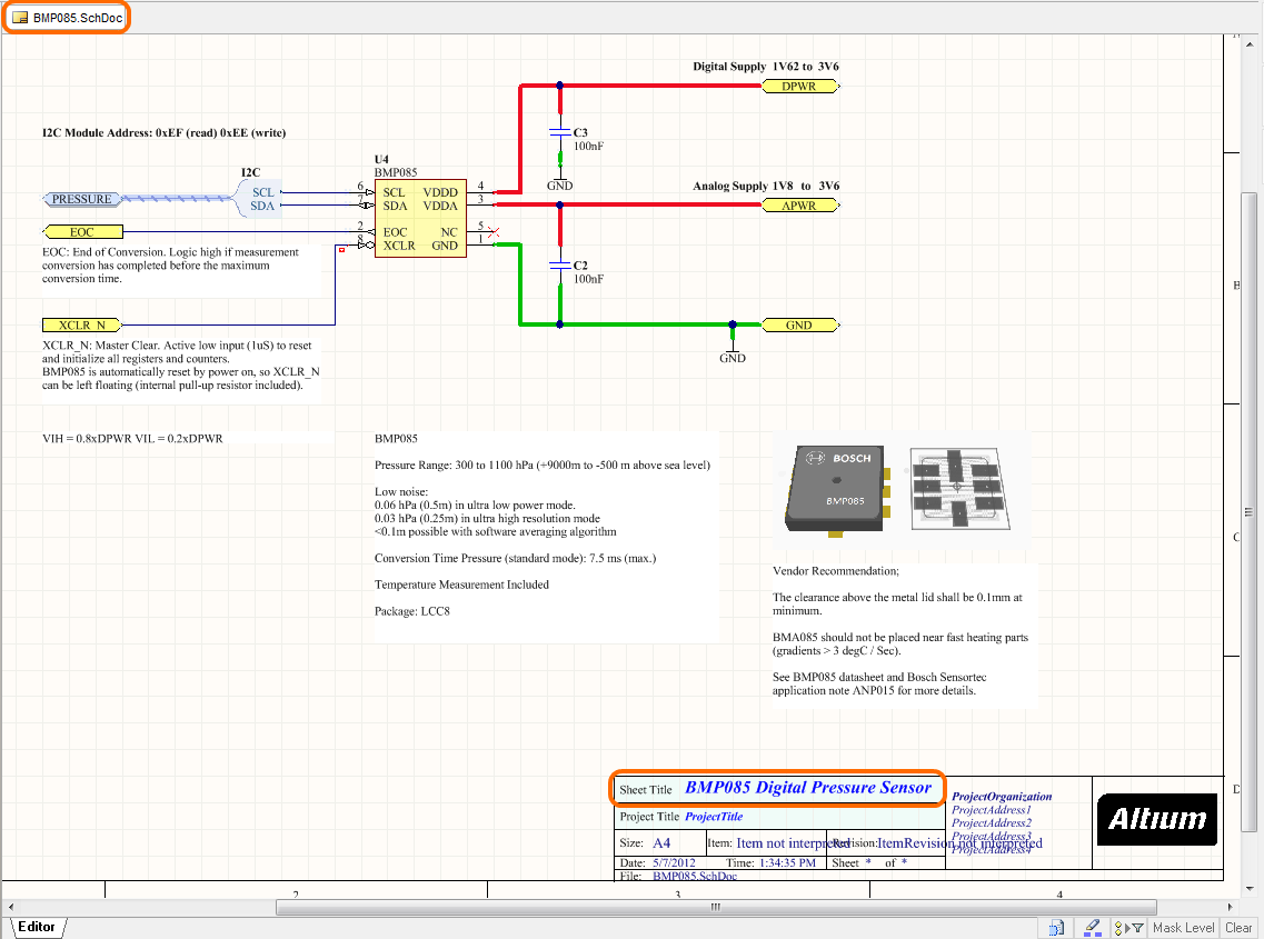
Example managed sheet, featuring a BMP085 component.
The filename is entered into the managed sheet Item's Comment field, while the sheet title is entered into its Description field – when creating the Item prior to release of the sheet itself. Coupled with using the same storage structure in both SVN and vault, a designer can quickly browse between the two and find either the design-side source or released design item. And having the filename appear as the Item's comment enables quick identification of what that managed sheet offers, in terms of key component and therefore circuit functionality.
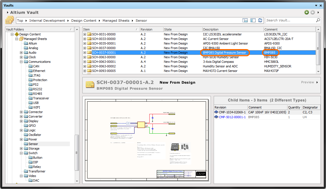
The schematic sheet's filename is used for the managed sheet item's comment, while the sheet title is used for the item's description.
Design Standards
When it comes to populating a blank schematic sheet, designers are rather chef-like in nature, each has their own signature way of doing things. Presentation-wise, for example, different designers will adopt different styles, layout preferences, use of color, and so on. After all, if all designers across the planet presented schematic circuitry in the exact same fashion, the design world would take on a mundane monochromatic-like appearance! So we will not look closely at the various presentation techniques implemented by the Team. The key is to adopt a method of capture and presentation that is consistent across your own design teams.
Now, in saying that, there are some key design principals that, when adopted, really do aid not only the consistency of the managed sheets produced, but are fundamental to the concept of design for reuse itself. The Hardware Team crank out managed sheets of reusable design circuitry, while adhering to the following overriding principles:
- Each managed sheet features a single or small group of key components focusing on a specific function.
- All possible supporting circuitry will be included in the sheet.
- Parts of the design that can be configured in multiple ways can be refactored to parent or sub-sheet within reason, allowing the sub-sheet behavior to be configured from the parent without adding unnecessary structural overhead.
- Multi-purpose signals are passed to parent sheets using reasonable and generic signal naming, allowing them to be re-mapped to their specific purpose.
- Ensure readability of the single standalone managed sheet is preserved, while allowing a designer to easily understand how it would be implemented as an element in their design.
- Use of consistent naming, presentation and design standards.
In terms of designing for reuse, the following items are implemented that are particularly relevant and important to capture at the managed sheet level:
- The use of signal harnesses where possible, since the standard harness is itself a reusable design element.
- No labeling of local nets – so avoiding the use of Net Labels – since doing so actually makes it harder to manage connectivity through the design in which the managed sheet is used. The most common exception to this however, is the requirement of such labeling when creating buses.
- All power ports connected to a port sheet interface and passed to the parent sheet – local power ports are avoided to prevent confusion.
- Port direction and I/O type is strictly set according to the signal direction with the exception of Power nets (these will be
unspecified). Where signal direction is not specified,Bidirectionalis used. - Using a standard set of signal names, using generic names where possible (e.g.
5V0instead of5.0V/5V/5Volts). There is a certain degree of flexibility here as well, since connections are explicit through the use of strict hierarchy across all design projects. This allows names to be defined differently for any two connected objects, at different levels of the design hierarchy, because their connection is explicit. - Using a standard set of sheet-level parameters.
Another addition to a managed sheet is that of a section to highlight the key component on the sheet, in terms of its manufacturer, and an at-a-glance listing of its key features. This can prove invaluable to a designer when assessing its merit for inclusion into a new design.
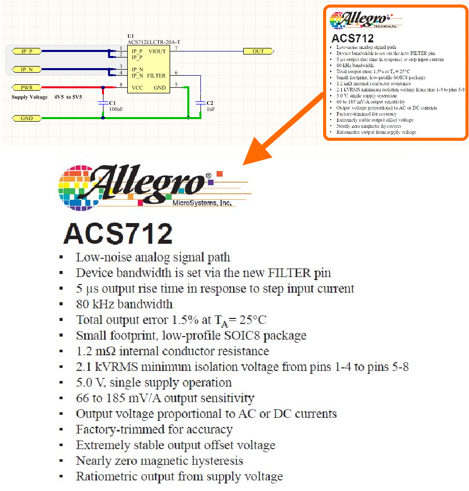
Features of the key component listed alongside the design circuitry.
Configuring and Releasing Designs
Related article: A Walk Through the Board Design Release Process
Once a design is considered ready for flight into the wider world, it needs to be released. Accommodating this, Altium Designer provides powerful, high-integrity board design release management, as part of Altium’s wider Design Data Management System. The board design release process is automated, enabling you to release configurations of your board design projects (and panel projects) without the risks associated with manual release procedures. When a particular project configuration is released, a snapshot of the design source is taken and archived along with any generated output. Release data is stored as revisions of a specific Item – the entity within a target Altium Vault, and which represents a tangible product that is made from that design project and sold by the company.
Using Standard Configurations
Related article: PCB Project Configurations
As part of the design methodology, a standard set of three configurations are predefined at the project template level for both standard board and panel projects – one for fabrication, one for assembly and one to essentially gather together all documentation. For each configuration, the relevant common output job configuration files are enabled for inclusion. The vault side of each configuration is left undefined. This further streamlines and reduces design effort, since the right configurations are in place for any future design project right from the start.
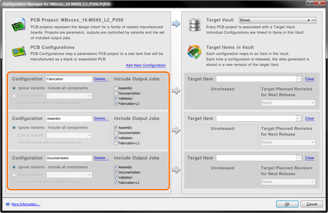
Default configurations defined as part of each template project ensure that correct (and consistent) output will be generated across any future design.
The Release Process
Related article: Releasing a Design with the PCB Release View
The release process itself is performed using Altium Designer's PCB Process Manager, the user-interface to which is provided courtesy of a dedicated view – the PCB Release view. Initiating the release is an automated affair, kicked off by pressing a single button. The process consists of several stages run in sequence – a process flow if you like. All stages in the process flow must run successfully, otherwise the release will fail and no data will be committed to the new Item Revision in the vault. As the process is fully automated, the risk of errors associated with a manual release process are no longer a consideration. Full validation, full checking. The data set for use by the supply chain is exactly what it needs to be, to produce the product exactly as you designed it
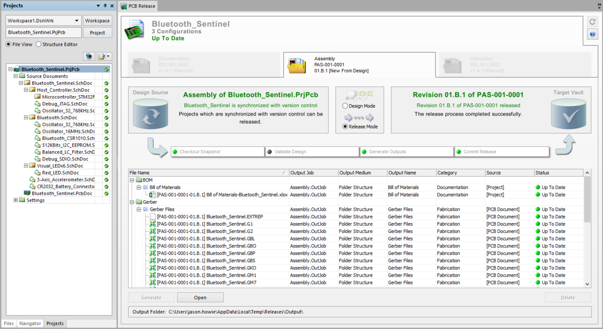
Successful release of a configuration of a design project using the PCB Release view! The release data (snapshot + outputs) is committed to the target vault, stored in the revision of the targeted Item.
The overall result is the highest-integrity board design release management possible. Not only is your actual design project tightly monitored, backed-up and managed in a version-controlled Design Repository, but also too, the releases of its configurations in a similar manner within the target Altium Vault – robust, safe, secure. And if the design itself is a satellite board to be used as part of a larger, parent design, then it exists in the vault ready to be used again and again – the very definition of designing for reuse!

Browsing the released board design item in the vault, courtesy of the Vaults panel.
Controlling Data Access
Related articles: Sharing Released Data through Publishing Destinations, Managing Access Rights for Revision Data
Direct access to data for a released PCB design project can be effectively controlled by a vault administrator through careful configuration of folder-level access permissions. However, this direct folder-level access to the data does not control which elements of the release data are accessible. So both the design snapshot AND the generated data are available. When interfacing to the manufacturer, only the fabrication and assembly "instructions" need to be shared, keeping the valuable design IP 'under wraps' as it were. And while a solution is available – to Publish only the data required by the Fabrication and Assembly Houses to fabricate and assemble the board respectively – this requires the involvement of dedicated Publishing Destinations.
A far better approach is to manage access to an Item Revision's data for a released PCB design – allowing users to see only the portion of data they are allowed to see, while by-passing the need for additional publishing. This is made possible through sharing at the individual Item Revision level, and the propagation of sharing permissions through to a revision's data folders (Released Documents and Design Snapshot). In this way, a standard set of sharing permissions can be defined at the Item level and passed through to its revisions, while having independent control over how the data for those revisions is shared.