SPICE Model Creation from User Data
Contents
- Accessing the Wizard
- Access in the Schematic Library Editor
- Access in the Schematic Editor
- Supported Device Types
- Naming the Model
- Characteristics to be Modeled
- Generating the Model
- Semiconductor Capacitor
- Semiconductor Resistor
- Current-Controlled Switch
- Voltage-Controlled Switch
- Lossy Transmission Line
- Uniform Distributed RC Transmission Line
- Diode
- Forward-bias current flow
- Reverse-bias junction capacitance
- Reverse-bias current flow
- Reverse recovery characteristics
- Bipolar Junction Transistor (BJT)
- Characteristics Modeled using Measured Data
- Forward-Bias Parameters
- Reverse-Bias Parameters
- Characteristics Modeled using Data from a Manufacturer's Data Sheet
- Forward-Bias Parameters
- Base-Emitter Voltage versus Collector Current
- Forward Early Voltage
- Characteristics Modeled using Measured or Manufacturer Data
- Base-Emitter Capacitance
- Base-Collector Capacitance
- Collector-Substrate Capacitance
- Transit Times
- Parameters not Extracted by the Wizard
In order to simulate a circuit design using Altium Designer's Mixed-Signal Circuit Simulator, all components in the circuit need to be simulation-ready – that is, they each need to have a linked simulation model.
The type of model and how it is obtained will largely depend on the component and, to some extent, on the personal preference of the designer. Many device manufacturer's supply simulation models corresponding to the devices they manufacture. Typically, it's as simple as downloading the required model file (SPICE, PSpice®) and hooking it up to the schematic component.
Some of the more basic analog device models in SPICE require no distinct model file – only specification of simple parameter values when defining the model link (e.g. Resistor, Capacitor). Attaching these types of models to a component is straigthforward and simply a process of select-and-enter (select the model type and enter the parameter values directly in an associated dialog).
Some models may need to be written from scratch – for example using the hierarchical sub-circuit syntax to create the required sub-circuit model file (*.ckt). Others – if the device is digital in nature – will require the device to be modeled using the proprietary Digital SimCode™ language, the definition of which is linked to through an intermediary model file.
Certain analog device models built-in to SPICE provide for an associated model file (*.mdl) in which to parameterically define advanced behavioral characteristics (e.g. Semiconductor Resistor, Diode, BJT). Creation of this model file by hand and then linking it manually to the required schematic component can be quite laborious. Not anymore – enter Altium Designer's SPICE Model Wizard. Using the Wizard the characetristics of such a device can be defined based on user-acquired data. The parameters – entered either directly or extracted from supplied data – are automatically written to a model file and that file linked to the nominated schematic component.
For more information on linking a model file, refer to the Linking a Simulation Model to a Schematic Component application note.
For detailed information on defining a digital simulation model, refer to the Creating and Linking a Digital SimCode Model application note.
The SPICE Model Wizard
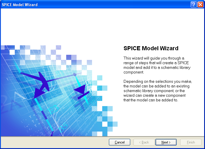
The SPICE Model Wizard provides a convenient, semi-automated solution to creating and linking a SPICE simulation model for a range of analog devices – devices that are built-in to SPICE, and that require a linked model file (*.mdl). The behavioral characteristics of the model are defined based on information you supply to the Wizard. The extent of this information depends on the device type you wish to create a model for – ranging from the simple entry of model parameters, to the entry of device data obtained from a manufacturer's data sheet or by measurements gained from the physical device itself.
The following sections discuss the use of the Wizard – from access to verification.
Accessing the Wizard
The way in which you access the Wizard depends chiefly on how you want to add the required SPICE model. A model can be added:
- To a newly created component (created by the Wizard) in a schematic library document
- To an existing component in a schematic library document
- To a placed component on a schematic document.
Access in the Schematic Library Editor
If you are unsure of the device you wish to model, access the Wizard by choosing Tools » XSpice Model Wizard from the main menus. By accessing the Wizard in this way, you will be able to choose:
- Which particular device you wish to model, from the list of supported device types (see Supported Device Types).
- Whether to add the subsequently-generated SPICE model to an existing component in the library document or to a new component that is created by the Wizard and added to that document.
The SPICE Model Wizard is essentially a collection of wizards - one per device model supported. This is made especially evident when accessing the Wizard from the Sim Model dialog.
- If you wish to add the model to an existing component, and have launched the Wizard using the main menu command, ensure that that component is the active component in the library.
You can also access the Wizard while setting up a simulation model link for an existing component. From the Sim Model dialog, simply ensure that the chosen entry in the Model Sub-Kind field is one of the device types supported by the Wizard (see Supported Device Types), then click on the Create button – to the right of the Model Name field (Figure 2).
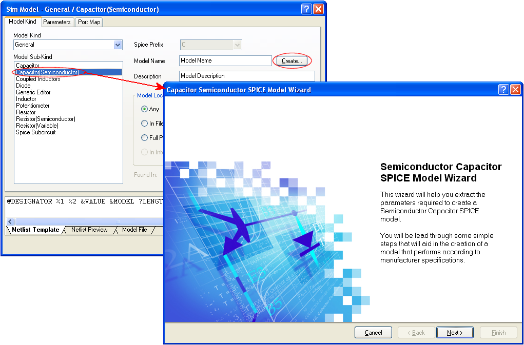
Figure 2. Access the Wizard directly from the Sim Model dialog.
The Sim Model dialog itself can be accessed from a schematic library document in one of the following ways:
- From the Library Component Properties dialog (Tools » Component Properties), by adding a simulation model in the Models region of the dialog. (Applies to the active component only).
If you are editing an existing linked simulation model, using the Wizard will replace the existing model with the newly created one.
- From the SCH Library panel, by adding a simulation model in the Models section of the panel. (Applies to the active component only).
- From the Schematic Library Editor's main design window, by adding a simulation model in the Models region of the window. (Applies to the active component only).
- From the Model Manager dialog (Tools » Model Manager), by adding a simulation model in the Models region of the dialog. (Applies to the selected component(s)).
Access in the Schematic Editor
Using the Wizard will replace any existing model with the newly created one.
The Wizard can also be accessed when defining the simulation model link for a placed component on a schematic sheet. Again, access is made from the Sim Model dialog by clicking the Create button – provided of course that the model type is one of those for which a dedicated Wizard is available.

Figure 3. Accessing the Wizard for a placed schematic component.
Supported Device Types
The Wizard can be used to create SPICE models for the following analog device types:
- Diode
- Semiconductor Capacitor
- Semiconductor Resistor
- Current-Controlled Switch
- Voltage-Controlled Switch
- Bipolar Junction Transistor (BJT)
- Lossy Transmission Line
- Uniform Distributed RC Transmission Line
Naming the Model
When using the Wizard to add a model to a new library component, the name specified for the model will be used to name the component also.
One of the most important steps as you follow the pages of the Wizard, is to provide a name for the model you are creating. In fact, you will not be able to proceed to the parameter definition stage of the Wizard until you have entered a name.
After creation, this name will appear in the Model Name field of the Sim Model dialog. The model file itself is also created using this name (ModelName.mdl).
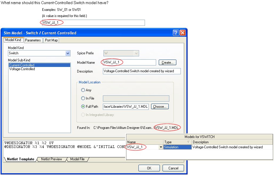
Figure 4. Define a meaningful name for the model.
When naming the model, you also have the option to enter a short description for it. This could be the function of the model (e.g. Semiconductor Resistor), or a more specific reference to a value or configuration (e.g. NPN BJT).
Characteristics to be Modeled
After giving the model a name, you will proceed to one or more pages dealing with the characteristics to be modeled. The model types supported by the Wizard can be categorized into the following two groups:
- Those models requiring direct entry of values for various model parameters. For further information, see the section Device Models Created by Direct Parameter Entry.
A parameter specified in the model file for a device will override its default value (inherent to the SPICE engine).
- Those models requiring the entry of data from which to extract the parameters that define the chosen device characteristics. The data entered is obtained either by direct measurement results from the physical device, or from a manufacturer's data sheet. For further information, see the section Device Models Created by Parameter Extraction from Data.
 Only parameters definable within a model file are considered by the Wizard. Any parameters that are definable at the component level for a device should be addressed using the Parameters tab of the Sim Model dialog, once the Wizard has finished creating the model file.
Generating the Model
After entry of the required data/parameters, the Wizard will display the generated model (Figure 5). This is the content that will be saved to the MDL file.
Figure 5. Previewing the generated model file content.
Editing of the model can be carried out directly on this page, giving you the utmost control over model specification.
Once you are satisfied with the model definition, simply click Next to pass to the end of the Wizard. Clicking Finish will allow you to save the model. Use the Save SPICE Model File dialog to determine where the resulting MDL file should be saved. By default, the file will be saved to the same directory as the schematic library document. You can also change the name of the file at this stage, should you wish.
If you have requested the model be attached to a new component, that component will be created and added to the library document.
Although the model is linked automatically to the component – new or existing – you should make a habit of verifying the mapping of schematic component pins to pins of the model. Simply access the Sim Model dialog for the attached model, click on the Port Map tab, and check the pin mapping – making any changes if required.
Figure 6. Verify the component-to-model mapping.
Define any additional parameters available for the model – on the Parameters tab of the Sim Model dialog – as required.
Device Models Created by Direct Parameter Entry
For the following device models the Wizard does not extract parameter information from entered data. Rather, the models are created based on direct entry of values for their associated parameters. When entering parameter values, there are a couple of things to bear in mind:
- If a value for a parameter is not specified, there will be no entry for it in the model file that is created. In this case, the default value stored internally in SPICE will be used. Put another way, if a value for a parameter is specified in a model file, then the model file value overrides that parameter's default value.
- If the default entry for a parameter in the Wizard is '-' and a value for that parameter is not specifically entered, a default value of zero will be used (internal to SPICE) for calculations.
Semiconductor Capacitor
The following parameters are definable for this device model, using the Wizard. Entering a value will cause that parameter to be written to the generated MDL file.
| CJ | Junction bottom capacitance (in F/meters2). | |
| CJSW | Junction sidewall capacitance (in F/meters). | |
| DEFW | Default device width (in meters). (Default = 1e-6). This value will be overriden by a value entered for Width on the Parameters tab of the Sim Model dialog. | |
| NARROW | Narrowing due to side etching (in meters). (Default = 0). |
For more information on this model type, refer to the SPICE3f5 Models.
Semiconductor Resistor
The following parameters are definable for this device model, using the Wizard. Entering a value will cause that parameter to be written to the generated MDL file.
| TC1 | First order temperature coefficient (in Ohms/˚C). (Default = 0) | |
| TC2 | Second order temperature coefficient (in Ohms/˚C2). (Default = 0) | |
| RSH | Sheet resistance (in Ohms). | |
| DEFW | Default width (in meters). (Default = 1e-6). This value will be overriden by a value entered for Width on the Parameters tab of the Sim Model dialog. | |
| NARROW | Narrowing due to side etching (in meters). (Default = 0). | |
| TNOM | Parameter measurement temperature (in ˚C). If no value is specified, the default value assigned to TNOM on the SPICE Options page of the Analyses Setup dialog will be used (Default = 27). |
For more information on this model type, refer to the SPICE3f5 Models.
Current-Controlled Switch
The following parameters are definable for this device model, using the Wizard. Entering a value will cause that parameter to be written to the generated MDL file.
| IT | Threshold current (in Amps). (Default = 0). | |
| IH | Hysteresis current (in Amps). (Default = 0). | |
| RON | ON resistance (in Ohms). (Default = 1). | |
| ROFF | OFF resistance (in Ohms). Default = 1/GMIN. GMIN is an advanced SPICE parameter, specified on the SPICE Options page of the Analyses Setup dialog. It sets the minimum conductance (maximum resistance) of any device in the circuit. Its default value is 1.0e-12 mhos, giving a default value for ROFF of 1000G Ohms. |
For more information on this model type, refer to the SPICE3f5 Models.
Voltage-Controlled Switch
The following parameters are definable for this device model, using the Wizard. Entering a value will cause that parameter to be written to the generated MDL file.
| VT | Threshold voltage (in Volts). (Default = 0). | |
| VH | Hysteresis voltage (in Volts). (Default = 0). | |
| RON | ON resistance (in Ohms). (Default = 1). | |
| ROFF | OFF resistance (in Ohms). By default this is set to 1/GMIN. GMIN is an advanced SPICE parameter setting, specified on the SPICE Options page of the Analyses Setup dialog. It sets the minimum conductance (maximum resistance) of any device in the circuit. its default value is 1.0e-12 mhos, therby giving a default value for ROFF of 1000G Ohms. |
For more information on this model type, refer to the SPICE3f5 Models.
Lossy Transmission Line
The following parameters are definable for this device model, using the Wizard. Entering a value (or setting a flag) will cause that parameter to be written to the generated MDL file.
| R | Resistance per unit length (in Ohms/unit). (Default = 0). | |
| L | Inductance per unit length (in Henrys/unit). (Default = 0). | |
| G | Conductance per unit length (in mhos/unit). (Default = 0). | |
| C | Capacitance per unit length (in Farads/unit). (Default = 0). | |
| LEN | Length of transmission line. |
| REL | Breakpoint control (in arbitrary units). (Default = 1). | |
| ABS | Breakpoint control (in arbitrary units). (Default = 1). | |
| NOSTEPLIMIT | A flag that, when set, will remove the restriction of limiting time-steps to less than the line delay. (Default = not set). | |
| NOCONTROL | A flag that, when set, prevents limiting of the time-step, based on convolution error criteria. (Default = not set). | |
| LININTERP | A flag that, when set, will use linear interpolation instead of the defaultquadratic interpolation, for calculation of delayed signals. (Default = not set). | |
| MIXEDINTERP | A flag that, when set, uses a metric for determining whether quadratic interpolation is applicable and, if it isn't, uses linear interpolation. (Default = not set). | |
| COMPACTREL | A specific quantity used to control the compaction of past history values used for convolution. By default, this quantity uses the value specified for the relative simulation error tolerance parameter (RELTOL), which is defined on the SPICE Options page of the Analyses Setup dialog. | |
| COMPACTABS | A specific quantity used to control the compaction of past history values used for convolution. By default, this quantity uses the value specified for the absolute current error tolerance parameter (ABSTOL), which is defined on the SPICE Options page of the Analyses Setup dialog. | |
| TRUNCNR | A flag that, when set, turns on the use of the Newton-Raphson iteration method to determine an appropriate time-step in the time-step control routines. (Default = not set, whereby a trial and error method is used – cutting the previous time-step in half each time). | |
| TRUNCDONTCUT | A flag that, when set, removes the default cutting of the time-step to limit errors in the actual calculation of impulse-response related quantities. (Default = not set). |
![]() For the resultant model to simulate, at least two of the R, L, G, C parameters must be given a value and also a value must be entered for the LEN parameter. You will not be able to proceed further in the Wizard until these conditions are met.
For the resultant model to simulate, at least two of the R, L, G, C parameters must be given a value and also a value must be entered for the LEN parameter. You will not be able to proceed further in the Wizard until these conditions are met.
For more information on this model type, refer to the SPICE3f5 Models.
Uniform Distributed RC Transmission Line
The following parameters are definable for this device model, using the Wizard. Entering a value will cause that parameter to be written to the generated MDL file.
| K | Propagation constant. (Default = 2). | |
| FMAX | Maximum frequency of interest (in Hertz). (Default = 1.0G). | |
| RPERL | Redsistance per unit length (in Ohms/meter). (Default = 1000). | |
| CPERL | Capacitance per unit length (in Farads/meter). (Default = 1.0e-15). | |
| ISPERL | Saturation current per unit length (in Amps/meter). (Default = 0). | |
| RSPERL | Diode resistance per unit length (in Ohms/meter). (Default = 0). |
For more information on this model type, refer to the SPICE3f5 Models.
Device Models Created by Parameter Extraction from Data
For Diode and BJT devices, the Wizard extracts parameter information from data you enter. The specific parameters extracted for inclusion in the model file will depend on the particular characteristics of the diode or BJT you have chosen to model.
The method of data entry varies between characteristics. In some cases, you will be required to enter direct data values, in others the entry of plot data. In any case all data will be sourced from direct device measurements, a manufacturer's data sheet, or a combination of the two.
For plot-based data, entering more data points will provide the Wizard with a truer 'picture' of the source data, which in turn leads to the greater accuracy of extracted parameter values.
When you are required to enter plot data, simply enter a series of data points obtained from the graphical source data, into the grid provided by the Wizard (Figure 7). If you have the data stored in comma separated value (*.csv) format, you can import the data using the available Import Data button. The Wizard will take the data you enter and use it to extract the required model parameters. The results of the extraction are presented on a subsequent page of the Wizard – in terms of the extracted parameter values themselves, and a comparison plot of the data entered and values calculated using the extracted parameters. Figure 7 illustrates an example of such a display of parameter results.
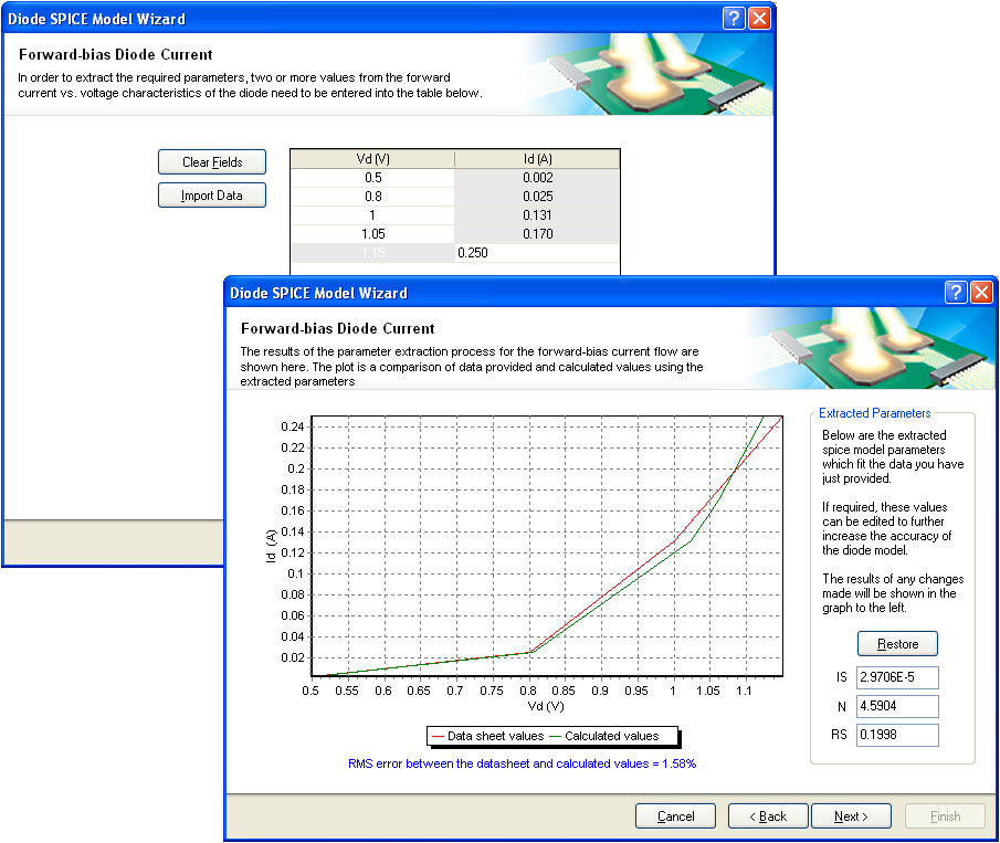
Figure 7. Enter source data for the Wizard to be able to extract the required model parameters.
You can edit the extracted parameter values to further refine the accuracy of the diode model. The graphical comparison will be updated to reflect the changes.
Diode
The following sections detail each of the characteristics that you can choose to model for a diode device. Each section discusses the parameters extracted and the source data required by the Wizard to facilitate their extraction.
For more information on this model type, refer to the SPICE3f5 Models.
Forward-bias current flow
The following parameters are used to describe the DC current-voltage characteristics of the diode in the forward-bias region:
| IS | Saturation current ( in Amps). | |
| N | Emission coefficient. | |
| RS | Ohmic resistance (in Ohms). |
To extract these parameters, a graph of the forward diode current (IF) versus the forward diode voltage (VF) is required. This graph can be obtained either from a manufacturer's data sheet or by measurements performed on a physical device.
Figure 8 shows an example of such a graph, obtained from a data sheet, and also an example test circuit, from which direct measurements could be taken to obtain the required source data.
Figure 8. Example graph and circuit for diode I-V characteristics in the forward-bias region.
Data is entered into the Wizard as a series of data points obtained from the source graph.
Reverse-bias junction capacitance
The following parameters are used to describe the capacitance of the diode when operating in the reverse-bias region:
| CJO | Zero-bias junction capacitance (in Farads). | |
| M | Grading coefficient. | |
| VJ | Junction potential (in Volts). |
To extract these parameters, a graph of the reverse-biased capacitance (Cd) versus the reverse diode voltage (VR) is required. This graph can be obtained either from a manufacturer's data sheet or by measurements performed on a physical device.
Figure 9 shows an example of such a graph, obtained from a data sheet, and also an example test circuit, from which direct measurements could be taken to obtain the required source data. The latter can be used if a capacitance meter is not available.
Figure 9. Example graph and circuit for diode capacitance in the reverse-bias region.
Data is entered into the Wizard as a series of data points obtained from the source graph.
The example circuit in Figure 9 is based on the equation:
I = C * (dv/dt).
Solving this equation for C gives:
C = I/(dv/dt).
The circuit produces a voltage ramp from the source V1. By calculating the slope of this ramp voltage the dv/dt part of the equation can be obtained. By taking the measured diode current and dividing it by the slope of the ramp voltage, the diode capacitance curve can be obtained.
Reverse-bias current flow
The following parameters are used to describe the after-breakdown, reverse-bias current flow of the device:
| BV | Reverse breakdown voltage (in Volts). | |
| IBV | Current at breakdown voltage (in Amps). |
To extract these parameters, the Wizard requires entry of the following two values:
- Value for the reverse breakdown voltage
- Value for the current through the diode at the point of reverse breakdown.
These values can be obtained either from a manufacturer's data sheet or by measurements performed on a physical device. Data sheets will typically contain the electrical (DC) characteristics of a diode in tabular format, so it is just a question of locating these values and entering them exactly as they are reported.
If the source data is graphical – typical of measurements taken directly from a physical device – you will need to 'read-off' these two values at the point where the diode begins to break down. Figure 10 shows an example of such a graph.

Figure 10. Graphically obtaining the current and voltage values at the reverse-breakdown point.
Although the values may be negative with respect to their display on the graph, when entered into the respective fields in the Wizard, they should be entered as positive values only.
Reverse recovery characteristics
The following parameter is used to model the reverse-recovery time of the diode while switching the diode from forward to reverse bias:
| TT | Transit time (in seconds). |
Direct measurement of this data is possible, but requires specialized equipment as the transit time of a diode can be as small as 1E-9s.
To extract this parameter, the Wizard requires entry of the reverse-recovery time of the diode (Trr), at the point where the forward current is equal to the reverse current (i.e. IR/IF=1). This data is typically found in the manufacturer data sheets for switching diodes in the form of simple numerical data.
Figure 11 illustrates the appearance of this information in a manufacturer's data sheet. The value of interest in Figure 11 – the entry to be made into the Wizard – is 4ns.
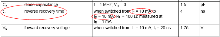
Figure 11. Obtaining the reverse-recovery time for a diode.
Bipolar Junction Transistor (BJT)
When creating a Bipolar Junction Transistor (BJT) model, the SPICE Model Wizard requires you to choose the source data from which the parameter information will be extracted:
- Measured Data – select this option if your source data comes from physical device measurements and you wish to develop an accurate model that describes all aspects of DC behavior.
- Manufacturer Data Sheet – select this option if your source data comes from a data sheet. Data sheets generally do not contain the level of information required to model all aspects of the BJT device. However, they will typically contain enough information to create a device model for use in the forward active region only.
When creating a BJT model, the Wizard also requires that you specify the transistor's polarity - NPN or PNP.
The differences between these two options mainly affect how the parameters modelling the DC current-voltage characteristics of the BJT are extracted. With respect to reverse-bias junction capacitances and transit times, the way in which the parameters are extracted are identical between the two.
The following sections detail each of the characteristics that you can choose to model for a BJT device, and in relation to the type of source data (measured data or data sheet). The parameters extracted in each case and the source data required by the Wizard to facilitate their extraction is discussed.
For more information on this model type, refer to the SPICE3f5 Models.
Characteristics Modeled using Measured Data
The following characteristics can be modelled when using data acquired from direct measurements made on the physical device.
Forward-Bias Parameters
The following parameters are used to describe the DC current-voltage characteristics of the BJT in the forward-bias region:
| IS | Transport saturation current (in Amps). | |
| BF | Ideal maximum forward beta. | |
| NF | Forward current emission coefficient. | |
| RB | Zero-bias base resistance (in Ohms). | |
| RC | Collector resistance (in Ohms). | |
| RE | Emitter resistance (in Ohms). | |
| IKF | Corner for forward beta high current roll-off (in Amps). | |
| ISE | B-E leakage saturation current (in Amps). | |
| NE | B-E leakage emission coefficient. | |
| VAF | Forward Early voltage (in Volts). |
The following sections detail the measurement data required, entry from which will enable the Wizard to extract these parameters.
Base-Emitter Voltage versus Base Current
This data is used for initial extraction of the RC parameter. Figure 12 shows an example graph of the Base-Emitter voltage (VBE) versus Base current (IB), and also an example test circuit, from which measurements could be taken to obtain the data. The circuit forces a current into the Base, while measuring the open-circuit base-emitter voltage.

Figure 12. Example graph and circuit for VBE vs. IB.
Data is entered into the Wizard as a series of data points obtained from the source graph.
Collector-Emitter Voltage versus Base Current
This data is used for initial extraction of the RE parameter. Figure 13 shows an example graph of the Collector-Emitter voltage (VCE) versus Base current (IB), and also an example test circuit, from which measurements could be taken to obtain the data. The circuit forces a current into the Base, while measuring the open-circuit Collector-Emitter voltage.
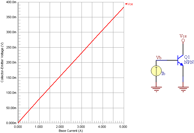
Figure 13. Example graph and circuit for VCE vs. IB.
Data is entered into the Wizard as a series of data points obtained from the source graph.
Forward Gummel Plot
This data is primarily used to extract the IS, BF, NF, RB, IKF, ISE and NE parameters. It is also used to optimize the RC, RE and VAF parameters. Figure 14 shows an example Gummel plot, and also an example test circuit, from which measurements could be taken to obtain the data. The Gummel plot illustrates:
- Base current versus Base-Emitter voltage (IB vs. VBE)
- Collector current versus Base-Emitter voltage (IC vs. VBE).
The Base-Collector voltage (VBC) is held at zero volts.
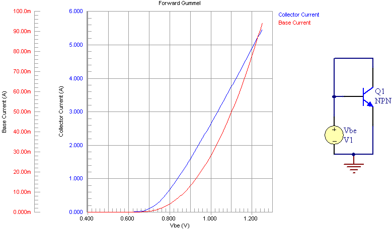
Figure 14. Example forward Gummel plot and test circuit.
Data is entered into the Wizard as a series of data points obtained from the source Gummel plot. The raw IB and IC values must be entered - the Wizard will apply the LN function to the curve data.
Collector Current versus Base-Emitter Voltage
This data is used for initial extraction of the VAF parameter. Figure 15 shows an example graph of the Collector Current (IC) versus Base-Emitter voltage (VBE), and also an example test circuit, from which measurements could be taken to obtain the data. The circuit is used to generate two curves of IC vs. VBE, for two different values of Base-Collector voltage (VBC). The curves should be measured at currents as low as possible and with VBC as close to zero volts as practical.
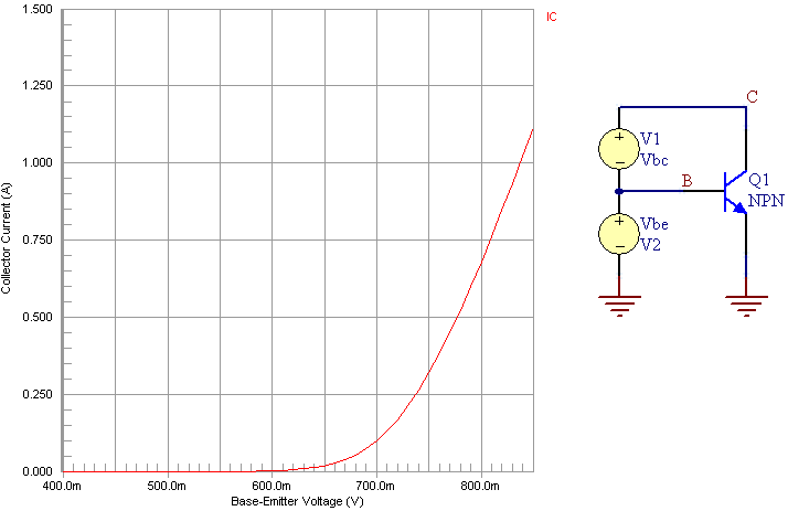
Figure 15. Example graphs and circuit for VBE vs. IC.
Data is entered into the Wizard as a series of data points into two tables – one for each source data curve. The value used for VBC also has to be entered in each case.
Reverse-Bias Parameters
The following parameters are used to describe the DC current-voltage characteristics of the BJT in the reverse-bias region:
| IS | Transport saturation current (in Amps). | |
| BR | Ideal maximum reverse beta. | |
| NR | Reverse current emission coefficient. | |
| RB | Zero-bias base resistance (in Ohms). | |
| RC | Collector resistance (in Ohms). | |
| RE | Emitter resistance (in Ohms). | |
| IKR | Corner for reverse beta high current roll-off (in Amps). | |
| ISC | B-C leakage saturation current (in Amps). | |
| NC | B-C leakage emission coefficient. | |
| VAR | Reverse Early voltage (in Volts). |
The following sections detail the measurement data required, entry from which will enable the Wizard to extract these parameters.
For information on the data required to extract the initial value for the RC parameter, see the previous section Base-Emitter Voltage versus Base Current.
For information on the data required to extract the initial value for the RE parameter, see the previous section Collector-Emitter Voltage versus Base Current.
Reverse Gummel Plot
This data is primarily used to extract the IS, BR, NR, RB, IKR, ISC and NC parameters. It is also used to optimize the RC, RE and VAR parameters. Figure 16 shows an example Gummel plot, and also an example test circuit, from which measurements could be taken to obtain the data. The Gummel plot illustrates:
- Base current versus Base-Collector voltage (IB vs. VBC)
- Emitter Current versus Base-Collector voltage (IE vs. VBC).
The Base-Emitter voltage (VBE) is held at zero volts.

Figure 16. Example reverse Gummel plot and test circuit.
Data is entered into the Wizard as a series of data points obtained from the source Gummel plot. The raw IB and IE values must be entered - the Wizard will apply the LN function to the curve data.
Emitter Current versus Base-Collector Voltage
This data is used for initial extraction of the VAR parameter. Figure 17 shows an example graph of the Emitter Current (IE) versus Base-Collector voltage (VBC), and also an example test circuit, from which measurements could be taken to obtain the data. The circuit is used to generate two curves of IE vs. VBC, for two different values of Base-Emitter voltage (VBE). The curves should be measured at currents as low as possible and with VBE as close to zero volts as practical.
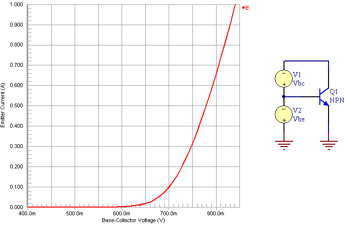
Figure 17. Example graphs and circuit for IE vs. VBC.
Data is entered into the Wizard as a series of data points into two tables – one for each source data curve. The value used for VBE also has to be entered in each case.
Characteristics Modeled using Data from a Manufacturer's Data Sheet
The following characteristics can be modelled when using data acquired from a manufacturer's data sheet.
Forward-Bias Parameters
The following parameters are used to describe the DC current-voltage characteristics of the BJT in the forward-bias region:
| IS | Transport saturation current (in Amps). | |
| BF | Ideal maximum forward beta. | |
| NF | Forward current emission coefficient. | |
| RE | Emitter resistance (in Ohms). | |
| IKF | Corner for forward beta high current roll-off (in Amps). | |
| ISE | B-E leakage saturation current (in Amps). | |
| NE | B-E leakage emission coefficient. |
The following sections detail the data required, entry from which will enable the Wizard to extract these parameters.
Base-Emitter Voltage versus Collector Current
Data sheets typically have these curves in a 'forced beta' or 'saturated' condition.
This data is used to extract the IS, NF, RE and IKF parameters. Figure 18 shows an example graph of the Base-Emitter voltage (VBE) versus the Collector current (IC), obtained from a data sheet.
Data is entered into the Wizard as a series of data points obtained from the source graph. The raw IC values must be entered - the Wizard will apply the LN function to the curve data.
The value for the forced beta ratio of the curve (β = IC/IB) also needs to be entered. In the example plot of Figure 18, this value is shown at the top-left of the graph, and so the value 10 would be entered.
DC Current Gain versus Collector Current
This data is used to extract the BF, NE, ISE and IKF parameters. Figure 19 shows an example graph of the DC current gain (hFE) versus the Collector current (IC), obtained from a data sheet.
Data is entered into the Wizard as a series of data points obtained from the source graph. For accuracy, values for the DC current gain should be entered for low, medium and high values of Collector current.
Forward Early Voltage
The following parameter is used to model the effect of base-width modulation in the Gummel-Poon transistor model:
| VAF | Forward Early voltage (in Volts). |
To extract this parameter you will need to enter a point from the Output Admittance (hOE) versus Collector current (IC) curve. Figure 20 shows an example of such a curve.
Simply read off any value on the curve. In the example of Figure 20, we can read off IC = 1mA and hOE = 30μmhos.
Typically, the data appears in tabular format, an example of which is shown in Figure 21.

Figure 21. Example tabular entry for Output Admittance.
The values of interest in Figure 21 – and the entries to be made in the Wizard – are 1mA for the Collector current and 30μmhos for the Output Admittance (the maximum value is typically used).
Characteristics Modeled using Measured or Manufacturer Data
Reverse-bias junction capacitance data is typically obtained from direct device measurements.
The following characteristics can be modelled when using data acquired from either a manufacturer's data sheet, or from direct measurements made on a physical device.
Base-Emitter Capacitance
The following parameters are used to describe the reverse-bias junction capacitance of the Base-Emitter junction:
| CJE | B-E zero-bias depletion capacitance (in Farads). | |
| MJE | B-E junction exponential factor. | |
| VJE | B-E built-in potential (in Volts). |
To extract these parameters, a graph of the reverse-biased B-E junction capacitance (Cj) versus the voltage characteristics (VBE) is required. If a capacitance meter is not available, the example test circuit of Figure 22 could be used to obtain the data. Figure 22 also shows example graphs obtained from such a circuit – plotting VBE and Cj against time respectively. From these graphs the values for VBE and Cj at corresponding points in time can be easily read-off.
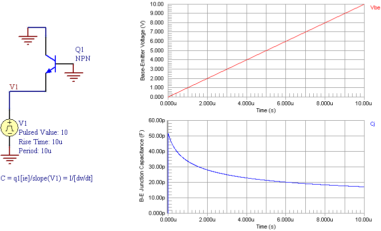
Figure 22. Example circuit and graphs for reverse-bias B-E junction capacitance.
Data is entered into the Wizard as a series of data points obtained from the source graph(s).
The example circuit in Figure 22 is based on the equation:
I = C * (dv/dt).
Solving this equation for C gives:
C = I/(dv/dt).
The circuit produces a voltage ramp from the source V1. By calculating the slope of this ramp voltage the dv/dt part of the equation can be obtained. By taking the measured diode current and dividing it by the slope of the ramp voltage, the diode capacitance curve can be obtained. The two graphs in Figure 22 relate to the circuit as follows:
- Top graph – VBE is V1
- Bottom graph – Cj is q1[ie]/(dV1/dt).
Base-Collector Capacitance
The following parameters are used to describe the reverse-bias junction capacitance of the Base-Collector junction:
| CJC | B-C zero-bias depletion capacitance (in Farads). | |
| MJC | B-C junction exponential factor. | |
| VJC | B-C built-in potential (in Volts). |
To extract these parameters, a graph of the reverse-biased B-C junction capacitance (Cj) versus the voltage characteristics (VBC) is required. If a capacitance meter is not available, the example test circuit of Figure 23 could be used to obtain the data. Figure 23 also shows example graphs obtained from such a circuit – plotting VBC and Cj against time respectively. From these graphs the values for VBC and Cj at corresponding points in time can be easily read-off.
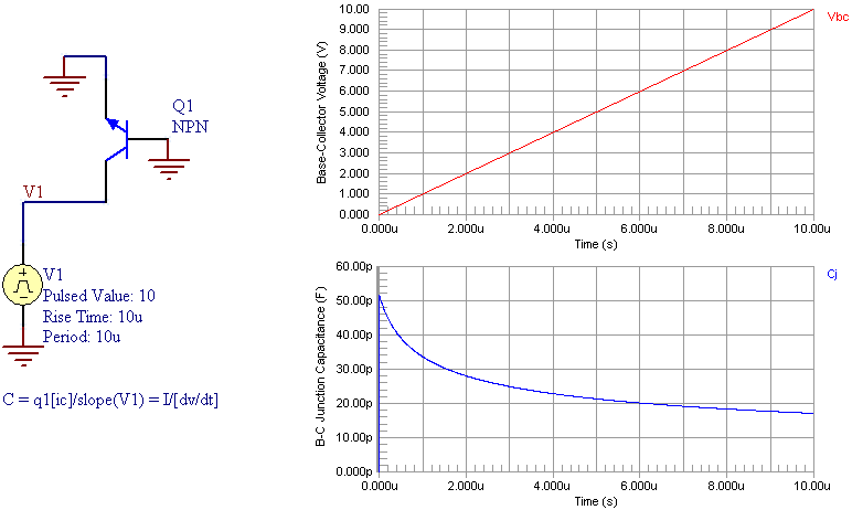
Figure 23. Example circuit and graphs for reverse-bias B-C junction capacitance.
Data is entered into the Wizard as a series of data points obtained from the source graph.
The example circuit in Figure 23 is based on the equation:
I = C * (dv/dt).
Solving this equation for C gives:
C = I/(dv/dt).
The circuit produces a voltage ramp from the source V1. By calculating the slope of this ramp voltage the dv/dt part of the equation can be obtained. By taking the measured diode current and dividing it by the slope of the ramp voltage, the diode capacitance curve can be obtained. The two graphs in Figure 23 relate to the circuit as follows:
- Top graph – VBC is V1
- Bottom graph – Cj is q1[ic]/(dV1/dt).
Collector-Substrate Capacitance
The following parameters are used to describe the reverse-bias junction capacitance of the Collector-Substrate junction:
| CJS | Zero-bias collector-substrate capacitance (in Farads). | |
| MJS | Substrate junction exponential factor. | |
| VJS | Substrate junction built-in potential (in Volts). |
To extract these parameters, a graph of the reverse-biased C-S junction capacitance (Cj) versus the voltage characteristics (VCS) is required. If a capacitance meter is not available, the example test circuit of Figure 24 could be used to obtain the data. Figure 24 also shows example graphs obtained from such a circuit – plotting VCS and Cj against time respectively. From these graphs the values for VCS and Cj at corresponding points in time can be easily read-off.

Figure 24. Example circuit and graphs for reverse-bias C-S junction capacitance.
Data is entered into the Wizard as a series of data points obtained from the source graph.
The example circuit in Figure 24 is based on the equation:
I = C * (dv/dt).
Solving this equation for C gives:
C = I/(dv/dt).
The circuit produces a voltage ramp from the source V1. By calculating the slope of this ramp voltage the dv/dt part of the equation can be obtained. By taking the measured diode current and dividing it by the slope of the ramp voltage, the diode capacitance curve can be obtained. The two graphs in Figure 24 relate to the circuit as follows:
- Top graph – VCS is V1
- Bottom graph – Cj is q1[is]/(dV1/dt).
Transit Times
The following parameters are used to describe the transit time of the BJT:
| TF | Ideal forward transit time (in seconds). | |
| TR | Ideal reverse transit time (in seconds). |
fT is typically listed in the small signal characteristics area of a data sheet, and is also referred to as the Current Gain - Bandwidth Product, or Unity-Gain Bandwidth.
To extract these parameters, the Wizard requires entry of the transistor's unity gain frequency (fT). This is the frequency at which the current gain of the transistor becomes unity. This data is typically found in manufacturer data sheets in the form of simple numerical data.
Figure 25 illustrates the appearance of this information in a manufacturer's data sheet. The value of interest in Figure 25 – the entry to be made into the Wizard – is 100MHz.
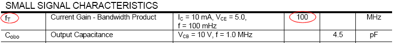
Figure 24. Access the Wizard directly from the Sim Model dialog.
Parameters not Extracted by the Wizard
The following parameters are difficult to extract from measurement data and are not usually present in manufacturer's data sheets. They are neither extracted by the Wizard nor added to the resulting model file for a BJT. Although not present in the MDL file, SPICE still uses these parameters when simulating the BJT device – using their inherent default values. These defaults are included below for ease of reference.
| IRB | Current where base resistance falls halfway to its minimum value (in Amps). (Default = infinite). | |
| RBM | Minimum base resistance at high currents (in Ohms). (Default = RB). | |
| XTF | Coefficient for bias dependence of TF. (Default = 0). | |
| VTF | Voltage describing VBC dependence of TF (in Volts). (Default = infinite). | |
| ITF | High-current parameter for effect on TF (in Amps). (Default = 0). | |
| PTF | Excess phase at freq=1.0/(TF*2PI)Hz (in Degrees). (Default = 0). | |
| XCJC | fraction of B-C depletion capacitance connected to internal base node. (Default = 1). | |
| XTB | Forward and reverse beta temperature exponent. (Default = 0). | |
| EG | Energy gap for temperature effect on IS (in eV). (Default = 1.11). | |
| XTI | Temperature exponent for effect on IS. (Default = 3). | |
| KF | Flicker noise coefficient. (Default = 0). | |
| AF | Flicker noise exponent. (Default = 1). | |
| FC | Coefficient for forward-bias depletion capacitance formula. (Default = 0.5). | |
| TNOM | Parameter measurement temperature (in ˚C). (The default value for this parameter is equal to the value entered for the TNOM parameter on the SPICE Options page of the Analysis Setup dialog. This entry is 27˚C by default). |
You can of course add any of these parameters into the MDL file, manually, specifying the values you wish to be used as required.