CLIMITERR - Controlled Limiter (Differential IO)

Model Kind
General
Model Sub-Kind
Generic Editor
SPICE Prefix
A
Model Name
CLIMIT
SPICE Netlist Template Format
@DESIGNATOR %%vd(%1,%2) %%vd(%3,%4) %%vd(%5,%6) %%vd(%7,%8) @"DESIGNATOR"CLIMIT
 .MODEL @"DESIGNATOR"CLIMIT climit (?in_offset|in_offset=@in_offset| ?gain|gain=@gain| ?upper_delta|upper_delta=@upper_delta| ?lower_delta|lower_delta=@lower_delta| ?limit_range|limit_range=@limit_range| ?fraction|fraction=@fraction|)
Parameters (definable at component level)
The following component-level parameters are definable for this model type and are listed on the Parameters tab of the Sim Model dialog. To access this dialog, simply double-click on the entry for the simulation model link in the Models region of the Component Properties dialog.
| In_Offset | input offset (Default = 0). |
| Gain | gain (default = 1). |
| Upper_Delta | output upper delta (Default = 0). |
| Lower_Delta | output lower delta (Default = 0). |
| Limit_Range | upper and lower smoothing range (Default = 1.0e-6). |
| Fraction | used to control whether the limit range is specified as a fractional (TRUE) or absolute (FALSE) value. (Default = FALSE). |
Notes
This model is similar in function to the Gain function. However, the output is restricted to the range specified by the output lower and upper limits, which are defined as follows:
Upper limit = value at device pin cntl_upper_p - value at device pin cntl_upper_n
Lower limit = value at device pin cntl_lower_p - value at device pin cntl_lower_n
The input signal can be either a differential current or differential voltage signal.
The Limit_Range is the value below the cntl_upper limit and above the cntl_lower limit at which smoothing of the output begins. A minimum positive value of current/voltage must exist between the cntl_upper and cntl_lower inputs, at all times. The Limit_Range therefore represents the delta, with respect to the output level, at which smoothing occurs. For example, for an input Gain of 2, Limit_Range of 0.1V and output limits of 1V (on pin cntl_upper) and -1V (on pin cntl_lower), the output will begin to smooth out at +/-0.9 V.
The input values arriving at the cntl_upper and cntl_lower pins of the device are tested to verify that they are far enough apart to guarantee a linear range between them. The range is calculated as:
(cntl_upper - Upper_Delta - Limit_Range) - (cntl_lower + Lower_Delta + Limit_Range)
and must be greater than or equal to zero.
When the Limit_Range is specified as a fractional value (Fraction parameter set to TRUE), it is expressed as the calculated fraction of the difference between cntl_upper and cntl_lower.
Examples
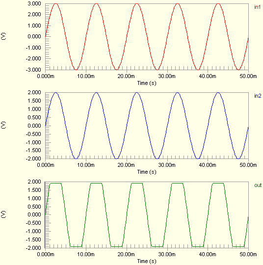
Consider the controlled limiter in the previous image, with the following characteristics:
- Pin1 (positive input) is connected to net
In1 - Pin2 (negative input) is connected to net
In2 - Pin3 (positive cntl_upper) is connected to net
Vuppos - Pin4 (negative cntl_upper) is connected to net
Vupneg - Pin5 (positive cntl_lower) is connected to net
Vlowpos - Pin6 (negative cntl_lower) is connected to net
Vlowneg - Pin7 (positive output) is connected to net
Out - Pin8 (negative output) is connected to net
GND - Designator is
U1 - Gain =
3 - All other model parameters are left at their inherent defaults
The entry in the SPICE netlist would be:
*Schematic Netlist:
 AU1 %vd(IN1,IN2) %vd(VUPPOS,VUPNEG) %vd(VLOWPOS,VLOWNEG) %vd(OUT,0) AU1CLIMIT
 .MODEL AU1CLIMIT climit ( gain=3    )
The effect of the function can be seen in the resultant waveforms obtained by running a transient analysis of the circuit.
In this example, the following analysis parameters on the Transient/Fourier Analysis page of the Analyses Setup dialog have been used:
- Transient Start Time - set to
0.000 - Transient Stop Time - set to
50.00m - Transient Step Time - set to
200.0u - Transient Max Step Time - set to
200.0u