ILIMITR - Current limiter (Differential IO)

Model Kind
General
Model Sub-Kind
Generic Editor
SPICE Prefix
A
Model Name
ILIMIT
SPICE Netlist Template Format
@DESIGNATOR %%vd(%1,%2) %%gd(%3,%4) %%gd(%5,%6) %%gd(%7,%8) @"DESIGNATOR"ILIMIT
 .MODEL @"DESIGNATOR"ILIMIT ilimit (?in_offset|in_offset=@in_offset| ?gain|gain=@gain| ?r_out_source|r_out_source=@r_out_source| ?r_out_sink|r_out_sink=@r_out_sink| i_limit_source=@i_limit_source i_limit_sink=@i_limit_sink ?v_pwr_range|v_pwr_range=@v_pwr_range| ?i_source_range|i_source_range=@i_source_range| ?i_sink_range|i_sink_range=@i_sink_range| ?r_out_domain|r_out_domain=@r_out_domain|)
Parameters (definable at component level)
The following component-level parameters are definable for this model type and are listed on the Parameters tab of the Sim Model dialog. To access this dialog, simply double-click on the entry for the simulation model link in the Models region of the Component Properties dialog.
| In_Offset | input offset (Default = 0). |
| Gain | gain (Default = 1). |
| R_Out_Source | sourcing resistance. The value entered must lie in the range 1.0e-9 to 1.0e9 (Default = 1). |
| R_Out_Sink | sinking resistance. The value entered must lie in the range 1.0e-9 to 1.0e9 (Default = 1). |
| I_Limit_Source | current sourcing limit. The value entered must be no lower than 1.0e-12. |
| I_Limit_Sink | current sinking limit. The value entered must be no lower than 1.0e-12. |
| V_Pwr_Range | upper and lower power supply smoothing range. The value entered must be no lower than 1.0e-15 (Default = 1.0e-6). |
| I_Source_Range | sourcing current smoothing range. The value entered must be no lower than 1.0e-15 (Default = 1.0e-9). |
| I_Sink_Range | sinking current smoothing range. The value entered must be no lower than 1.0e-15 (Default = 1.0e-9). |
| R_Out_Domain | internal/external voltage delta smoothing range. The value entered must be no lower than 1.0e-15 (Default = 1.0e-9). |
Notes
This function models the operation of an operational amplifier or comparator, at the highest level. All of the device pins act as inputs, with six of the eight - pos-pwr, neg-pwr and out pin pairs (differential) - also capable of acting as outputs.
The device takes a differential voltage input and applies offset and gain, as determined by the values assigned to the In_Offset and Gain parameters. An equivalent internal voltage (VEq) is derived from the result, which is subsequently limited by the range defined by the differential voltages applied to the pos_pwr and neg_pwr pins. If VEq is greater than the subsequent voltage that appears on the out pin of the device, a sourcing current flows from the out pin. If the value for VEq is less than that seen on the out pin, a sinking current flows into the out pin.
If a sourcing current results, the value of the current will be controlled by a sourcing resistance, as defined by the R_Out_Source parameter. The sourcing current is limited to a maximum value defined by the I_Limit_Source parameter. The output current in this case will be reflected in the current through the pos_pwr pins of the device.
If a sinking current results, the value of the current will be controlled by a sinking resistance, as defined by the R_Out_Sink parameter. The sinking current is limited to a maximum value defined by the I_Limit_Sink parameter. (This models the limiting behavior found in the output stages of most operational amplifiers). The output current in this case will be reflected in the current through the neg_pwr pins of the device.
The V_Pwr_Range parameter is used to define the voltage level below Vpos_pwr and above Vneg_pwr , beyond which smoothing will be applied to the derived internal voltage signal, VEq.
The I_Source_Range parameter is used to define the current level below I_Limit_Source, beyond which smoothing is applied. This value also determines the current increment above Iout = 0, at which the current through the pos_pwr pins begins to transition to zero.
The I_Sink_Range parameter is used to define the current level below I_Limit_Sink, beyond which smoothing is applied. This value also determines the current increment below Iout = 0, at which the current through the neg_pwr pins begins to transition to zero.
The R_Out_Domain parameter is used to specify the incremental value above and below (VEq - Vout ) = 0, at which Rout will be set to R_Out_Source or R_Out_Sink respectively. Rout will be interpolated smoothly between R_Out_Source and R_Out_Sink under the following condition:
-R_Out_Domain < (VEq - Vout ) > R_Out_Domain
Examples
Consider the current limiter in the above image, with the following characteristics:
- Pin1 (positive input) is connected to net
In1 - Pin2 (negative input) is connected to net
In2 - Pin3 (positive pos_pwr input) is connected to net
Vpospwr+ - Pin4 (negative pos_pwr input) is connected to net
Vpospwr- - Pin5 (positive neg_pwr input) is connected to net
Vnegpwr+ - Pin6 (negative neg_pwr input) is connected to net
Vnegpwr- - pin7 (positive output) is connected to net
Out - Pin8 (negative output) is connected to net
GND - Designator is
U1 - Gain =
2 - I_Limit_Source =
3mA - I_Limit_Sink =
3mA - All other model parameters are left at their inherent default values
The entry in the SPICE netlist would be:
*Schematic Netlist:
 AU1 %vd(IN1,IN2) %gd(VPOSPWR+,VPOSPWR-) %gd(VNEGPWR+,VNEGPWR-) %gd(OUT,0)
 + AU1ILIMIT
 .MODEL AU1ILIMIT ilimit ( gain=2   i_limit_source=3mA i_limit_sink=3mA    )
The effect of the function can be seen in the resultant waveforms obtained by running a transient analysis of the circuit.
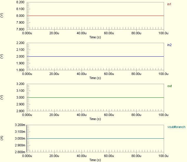
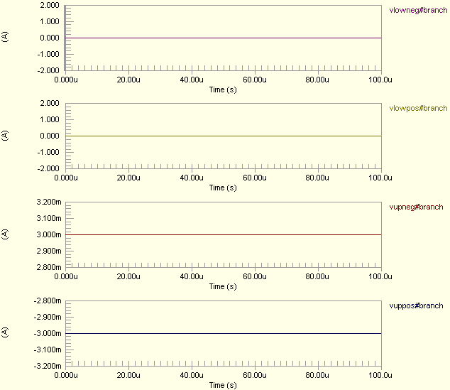
In this example, the following analysis parameters on the Transient/Fourier Analysis page of the Analyses Setup dialog have been used:
- Transient Start Time - set to
0.000 - Transient Stop Time - set to
100.0u - Transient Step Time - set to
20.00n - Transient Max Step Time - set to
20.00n