Via
Parent page: Objects
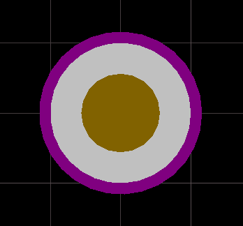
A via that spans and connects from the top layer (red) to the bottom layer (blue), and also connects to one internal power plane (green).
Summary
A via is a primitive design object. It is used to form an electrical connection between two or more electrical layers of a PCB. Vias are a 3 dimensional object, having a barrel-shaped body in the Z-plane (vertical), with a flat ring on each (horizontal) copper layer. The barrel-shaped body of the via is formed when the board is drilled and through-plated during fabrication. In the X and Y planes vias are circular, like round pads. The key difference between a via and a pad is that as well as being able to span all layers of the board (top to bottom), a via can also span from a surface layer to an internal layer, or between two internal layers.
Availability
Vias are available for placement in both the PCB editor and the PCB Library editor:
PCB Editor
- Click Place » Via.
- Click button
 in Wiring toolbar.
PCB Library Editor
- Click Place » Via.
- Click button in Wiring toolbar.
Placement
After launching the command, the cursor will change to a crosshair and you will enter via placement mode:
- Position the cursor and click or press Enter to place a via.
- Continue placing further vias, or right-click or press Esc to exit placement mode.
Auto-placement of Vias During Routing
When a net is being interactively routed, you can cycle through the available signal layers by pressing the * key on the numeric keypad. When this is done the software will automatically place a via, in accordance with the applicable Via Style design rule. Note that multiple Via Style design rules can be defined, allowing different via sizes to be assigned to different nets.
Default Settings versus Design Rules
When a via is placed in free space, it is not possible for the software to apply the design rules during placement. In this situation the default via will be placed, as defined in the PCB - Defaults page of the Preferences dialog.
Non-Graphical Editing...
The following methods of non-graphical editing are available:
...via an Associated Properties Dialog
This method of editing uses the following dialog to modify the properties of a via object.
Edit the properties of the Via in the dialog.
The Via dialog can be accessed prior to entering placement mode, from the PCB Editor – Defaults page of the Preferences dialog. This allows the default properties for the via object to be changed, which will be applied when placing subsequent vias.
During manual via placement, the dialog can be accessed by pressing the Tab key.
After placement, the dialog can be accessed in one of the following ways:
- Double-clicking on the placed via object.
- Placing the cursor over the via object, right-clicking and choosing Properties from the context menu.
- Click Edit » Change, then click an existing object.
Thru-hole, Blind and Buried Vias
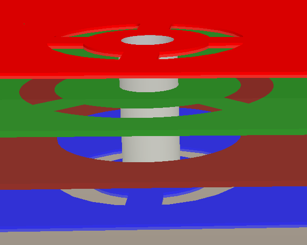
The default is for a via to span from the Top Layer through to the Bottom Layer - this is known as a thru-hole via. In a multilayer board a via can also span other layers. The possible layers that a via can span depends on the fabrication technology used to fabricate the board. The traditional approach to manufacture a multi-layer board was to make it as a set of thin double-sided boards, which are then sandwiched together under heat and pressure to form a multi-layer board.
The image below shows a 6 layer board, as shown by the layer names down the left of the image. This board would first be fabricated as 3 double-sided boards (Top-Plane1, Mid1-Mid2, Plane2-Bottom), as indicated by the hatched core layers.
These double-sided boards can have via sites drilled if required, forming what are known as blind vias (via number 1) when the via spans from a surface layer to an inner layer; and buried vias, when a via spans from one internal layer to another internal layer (via number 2). After the layers are pressed together into a single multi-layer board, thru-hole vias are drilled (via number 3).
Another type of multi-layer board fabrication technology is call Build-up technology, where layers are added one after the other, often over a double-sided or traditional multi-layer board. When this technology is used vias can be drilled with a laser after each layer is added during the build up process, resulting in a large number of possible layer-pairs that can be spanned. The layer-pairs used for each via is defined by the Start Layer and End Layer settings for the via. If blind, buried or build-up type vias are to be used, the Drill pairs must be configured.
Configuring the Layer Drill Pairs
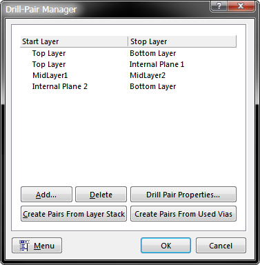
When blind, buried or build-up type vias are to be used, the Drill pairs must be configured. This ensures that when the fabrication output files are generated from the completed board, there are suitable drill files for the various drill jobs that must be performed to create the blind or buried vias. Drill Pairs are configured in the Drill Pair Manager dialog, as shown in the image below. To open the dialog first open the Layer Stack Manager dialog (click Design » Layer Stack Manager), then click the Drill Pairs button to open the Drill Pair Manager dialog.
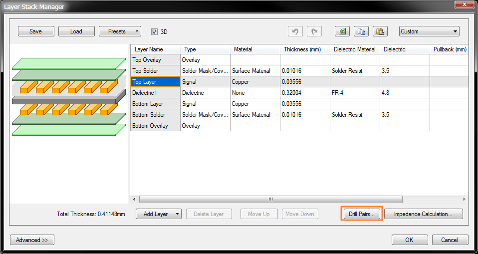
The arrangement of the copper layers is defined in the Layer Stack Manager. From there the Drill Pair Manager can be opened to define the required drill pairs.
Solder Mask Expansion
The Solder Mask Expansions defines the amount of opening in the Solder Mask layer, measured from the edge of the via to the edge of the opening in the mask. The default setting for a via is to use the Expansion value from the rules, which means the expansion is specified by the applicable Solder Mask Expansion design rule. This can be overridden for each individual via if required by enabling the Specify expansion value option, and entering a suitable numeric value (positive or negative).
The opening in the Solder Mask can also be completely closed if required, by enabling the required Force complete tenting on top/bottom options. Note that tenting a via means it cannot be used as a Testpoint on that side of the board.
Testpoint Settings
Each via (or pad) can be used as a testpoint site, on the top, bottom or both sides of the board by enabling the required Testpoint Settings. Testpoint locations are included in the Testpoint Report, click File » Fabrication Outputs » Test Point Report or File » Assembly Outputs »Test Point Report to generate this report.
...via an Inspector Panel
An Inspector panel enables the designer to interrogate and edit the properties of one or more design objects in the active document. Used in conjunction with appropriate filtering, the panel can be used to make changes to multiple objects of the same kind, from one convenient location.
...via a List Panel
A List panel allows the designer to display design objects from one or more documents in tabular format, enabling quick inspection and modification of object attributes. Used in conjunction with appropriate filtering, it enables the display of just those objects falling under the scope of the active filter – allowing the designer to target and edit multiple design objects with greater accuracy and efficiency.
Graphical Editing
Vias cannot have their properties modified graphically, other than their location.
- To move a via without moving the connected tracks, click, hold and move the via.
- To move a via and also move the connected tracks, click once to select it, then click a second time (do not hold) and move the via. The connected routing will remain attached to the via as it is moved.