Pad
Parent page: Objects


Pads are used to provide both mechanical mounting and electrical connections to the component pins.
Summary
A pad is a primitive design object. Pads are used to create the interconnection points from the component pins to the routing on the board. Pads can be used individually as free pads in a design, or more typically, they are used in the PCB Library Editor, where they are incorporated with other primitives into component footprints.
Availability
Pads are available for placement in both the PCB editor and the PCB Library editor:
PCB Editor
- Click command Place » Pad from main menu.
- Click button
 from Wiring toolbar.
PCB Library Editor
- Click command Place » Pad from main menu.
- Click button from PCB Lib Placement toolbar.
Placement
After launching the command, the cursor will change to a crosshair and you will enter pad placement mode.
- Position the cursor and click or press Enter to place a pad.
- Press the Tab key to access an associated properties dialog, from where properties for the region can be changed on-the-fly.
- Continue placing further pads, or right-click or press Esc to exit placement mode.
Non-Graphical Editing...
The following methods of non-graphical editing are available:
...via an Associated Properties Dialog
This method of editing uses the following dialog to modify the properties of a pad object.
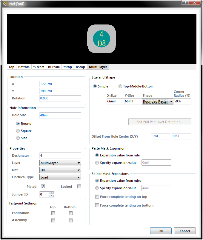
Edit the properties of the Pad in the dialog.
The Pad dialog can be accessed prior to entering placement mode, from the PCB Editor – Defaults page of the Preferences dialog. This allows the default properties for the pad object to be changed, which will be applied when placing subsequent pads.
During placement, the dialog can be accessed by pressing the Tab key.
After placement, the dialog can be accessed in one of the following ways:
- Double-clicking on the placed pad object.
- Placing the cursor over the pad object, right-clicking and choosing Properties from the context menu.
- Run command Edit » Change, then click an existing object.
Size and Shape
The Size and Shape properties allow you to choose between 3 different configurations of pad:
- Simple - the size and shape of the pad is the same on all signal layers.
- Top-Middle-Bottom - the size and shape can be uniquely defined for the top layer, all mid layers as a set, and the bottom layer.
- Full Definition - the size and shape can be uniquely defined for all signal layers.
There are 4 Shapes available:
- Round - a circular shaped pad.
- Rectangular - a square or rectangular shaped pad (depending on the X-Size and Y-Size), the corners are 90 degrees.
- Rounded Rectangle - a square or rectangular shaped pad, the corners are rounded by the amount defined in the Corner Radius setting. The Corner Radius is defined as a percentage of the shortest edge of the pad, where 0% results in 90 degree corners and 100% results in a circular pad if the X-Size and Y-Size are the same (the rounded corner extends half way along the pad edge).
- Octagonal - an eight-sided pad.
Hole Information
Hole Size - the size specified is the drill size rather than the finished hole size.
Three pad hole types are supported, Round, Slot and Square.
- Round - holes are drilled.
- Slot - slot holes have rounded ends and are typically milled.
- Square - square holes are intended to be punched.
When NC Drill output is generated, there is a separate file created for each hole type.
Designator
Each pad should be labeled with a designator, which is usually a component pin number. The designator can be up to 20 alphanumeric characters in length. Pad designators will auto-increment by 1 during placement if the initial pad has a designator ending with a numeric character. Press Tab to change the designator of the first pad prior to placement. To achieve alpha or numeric designator increments other than 1, use the Paste Array feature. Controls for this feature are provided in the Setup Paste Array dialog, accessed by pressing the Paste Array button in the Paste Special dialog (click Tools » Paste Special).
Use the Paste Array feature to automatically define suitable pad designators.
By setting the Designator of the pad prior to copying it to the clipboard and setting the Text Increment field in the Setup Paste Array dialog, the following types of pad designator sequences can be placed:
- Numeric (eg. 1, 3, 5) - to increment numerically, set the Text Increment field to the amount you wish to increment by.
- Alphabetic (eg. A, B, C) - To increment alphabetically, set the Text Increment field to the letter in the alphabet that represents the number of letters you wish to skip. For example, if the initial pad had a designator of 1A and the Text Increment field was set to C, the pads placed would have the designators 1A, 1D, 1G and so on.
- Alphanumeric (eg. A1, A2; 1A, 1B; A1, B1; 1A, 2A, etc)
Layer
The layer that the pad is present on. When designing a surface mount component footprint, set the layer to Top layer even if the component is intended to be used on the bottom side of the board. The software will automatically flip the pads' layer when the component is flipped to the bottom side of the board.
Net
Name of the net that this pad connects to.
Jumper ID
If it is not physically possible (or desirable) to implement all connections as routing, for example on a single-sided PCB, then jumpers can be used. Within a component footprint, label the pads that are to be connected by a jumper with the same Jumper ID value. Pads that share the same Jumper ID and Net name tell the system that these pins will be connected by a physical jumper during PCB assembly.
Jumper connections are shown as curved connection lines in the PCB Editor. The Design Rules Checker will not report jumper connections as unrouted nets.
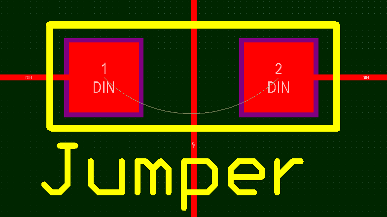
Wire-link style jumpers can be defined by setting matching JumperID values in both pads.
Testpoint Settings
Each pad (or via) can be used as a testpoint site, on the top, bottom or both sides of the board by enabling the required Testpoint Settings. Testpoint locations are included in the Testpoint Report, click File » Fabrication Outputs » Test Point Report to generate this report.
Paste Mask Expansion
The Paste Mask Expansions defines the amount of opening in the Paste Mask layer, measured from the edge of the pad to the edge of the opening in the mask. The default setting for a pad is to use the Expansion value from the rules, which means the expansion is specified by the applicable Paste Mask Expansion design rule. This can be overridden for each individual pad if required by enabling the Specify expansion value option, and entering a suitable positive or negative numeric value to open or close the mask as required.
Solder Mask Expansions
The Solder Mask Expansions defines the amount of opening in the Solder Mask layer, measured from the edge of the pad to the edge of the opening in the mask. The default setting for a pad is to use the Expansion value from the rules, which means the expansion is specified by the applicable Solder Mask Expansion design rule. This can be overridden for each individual pad if required by enabling the Specify expansion value option, and entering a suitable positive or negative numeric value to open or close the mask as required.
The opening in the Solder Mask can also be completely closed if required, by enabling the required Force complete tenting on top/bottom options. Note that tenting a pad means it cannot be used as a Testpoint on that side of the board.
...via an Inspector Panel
An Inspector panel enables the designer to interrogate and edit the properties of one or more design objects in the active document. Used in conjunction with appropriate filtering, the panel can be used to make changes to multiple objects of the same kind, from one convenient location.
...via a List Panel
A List panel allows the designer to display design objects from one or more documents in tabular format, enabling quick inspection and modification of object attributes. Used in conjunction with appropriate filtering, it enables the display of just those objects falling under the scope of the active filter – allowing the designer to target and edit multiple design objects with greater accuracy and efficiency.
Graphical Editing
Pads cannot have their properties modified graphically, other than their location.
- To move a free pad and also move the connected tracks, click, hold and move the pad. The connected routing will remain attached to the pad as it is moved.
- To move a free pad without moving the connected tracks, in the PCB or PCB Library Editor use the Edit » Move » Move command, then click on the required pad (effectively picking it up), and move to the required new position, clicking again to drop.