Component
Parent page: Objects
The component footprint defines the component mounting and connections on the PCB, and can also include 3D body objects to define the actual component.
Summary
The component footprint defines the space and connection points needed to mount the physical component on the printed circuit board. It is made up of a collection of simple primitive objects, which could include pads, lines and arcs. The pads provide the mounting and connection points for the component pins. Additional design primitives, such as lines and arcs, are often included to define the outline of the component shape on the component overlay (silkscreen) layer.
The component footprint can also include optional 3D body objects which define the physical space or envelope of the actual component that is mounted on the board. By defining the physical component using 3D body objects, 3 dimensional component clearance checking can be performed.
Availability
Component footprints are created in the PCB Library editor, and placed in the PCB editor. To place a component in the PCB editor:
- Click Place » Component
- Locate the component in the Libraries panel (System » Library), and click the Place <ComponentName> button.
- From within an open PCB Library, click Tools » Update PCB with All Footprints and select Place Component in PCB to place the current component into the last active PCB document.
Placement
The process used to locate the required component footprint will depend on the method chosen to perform placement. Once the required footprint has been chosen for placement and is floating on the cursor:
- Press Tab to edit the properties of the component before it is placed.
- Press Spacebar to rotate the component anti-clockwise (Shift+Spacebar for clockwise). The default rotation step is 90 degrees, to change this set the Rotation Step value in the PCB Editor - General page of the Preferences dialog.
- If the component is being rotated, the default behavior is for the Designator and Comment strings is to rotate with the footprint. This behavior is controlled by the Autoposition setting for these strings, the defaults can be set by editing the default Component in the PCB Editor - Defaults page of the Preferences dialog. Note that setting the default will not affect any components that have already been placed.
- Press the L shortcut to flip the component to the bottom side of the board. Do not use the X or Y keys as this will mirror the part but not change its layer.
Placing From the Menu
To place from the menu:
- Click Place » Component, the Place Component dialog will open, as shown below.
- If the footprint name is know, type it into the Footprint field (it must exactly match the actual footprint name).
- Enter a suitable Designator, and include a footprint Comment if required.
- Click OK, the footprint will appear floating on the cursor, ready for placement.
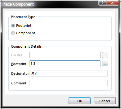
Use the Place Component dialog when the Footprint name is known.
If the exact footprint name is not known:
- Click the
 button beside the Footprint field in the Place Component dialog to open the Browse Libraries dialog, as shown below.
 - Select the required library in the Libraries dropdown, and Mask or scroll to locate the required footprint.
- Select the component and click OK to return to the Place Component dialog and continue with the placement.
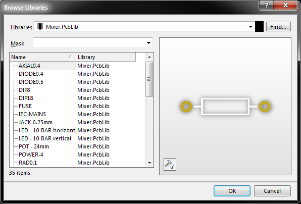
The Browse Libraries dialog includes a display of the selected footprint, allowing you to visually select the correct component.
Placing From the Libraries Panel
To place from the Libraries panel:
- The default setting is to only show schematic libraries in the panel, to enable PCB libraries click the next to the chosen library field, and enable Footprints for browsing, as shown below.
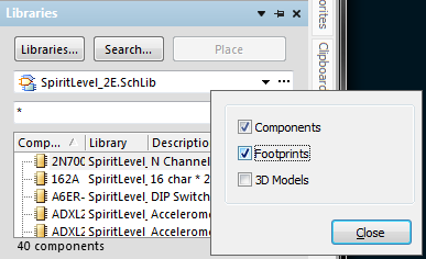
Enable PCB libraries for browsing in the Libraries panel.
Once footprint libraries have been enabled:
- Use the dropdown next to the library name to choose the required footprint library for browsing. In the image below the SpiritLevel pcb library has been chosen.
- Use the mask field (below the currently selected library field) to filter the list and speed the searching process, or scroll and select the required part.
- Click the Libraries button to open the Available Libraries dialog and add or remove libraries.
- Click the Search button to open the Libraries Search dialog and search for a component footprint.
- Click the Place button, double-click, or click and drag to place the selected component into the workspace.
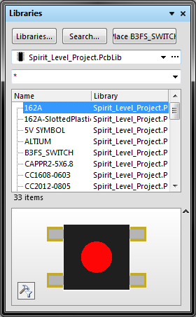
The selected component is ready for placing from the Libraries panel.
Searching for a Component Footprint
If you cannot locate the required component footprint in the Libraries panel, use the Search feature. To do this, click the Search button to open the Libraries Search dialog (as shown below).
Note that:
- The default search Scope is to search for Footprints in the Available Libraries (as shown by the Scope options in the image below).
- Alternatively, the Libraries Search dialog also supports searching through Libraries on a path, stored in folders on a drive. To do this enable the Libraries on Path option, then configure the Path options as required.
- The Filters are logically AND'ed, it can be better to start with a simpler filter and then if there are many results, use the Refine last search mode to search within the results.
- Search results are presented in the Libraries panel, clustered under Query Results. If the footprint you choose in the Query Results is from a library that is not currently available, the software will prompt to install the library (note that this feature is not available if you click and drag to place). Re-select a footprint library to return to browsing in the panel.
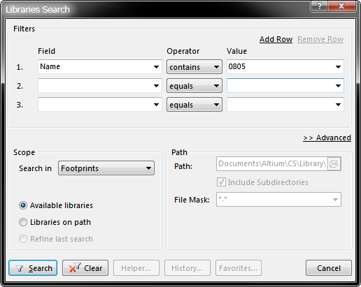
Search for the footprint in the Available libraries, or search Libraries on a path.
Placing from the Library Editor
A component can also be placed directly from a library that is open the PCB Library editor. This is done from the PCB Library panel, as shown below. If the panel is not visible, click System » Libraries to enable it.
Note that:
- Click Tools » Update With All Footprints and select Place Component in PCB to place the current component into the last active PCB workspace.
- Alternatively, right-click and select Place from the PCB Library panel context menu.
- While the part is floating on the cursor, it can be edited (press Tab), rotated (press Spacebar), or flipped to the other side of the board (press L) before placement.
- If a part is placed directly from a library, that library does not need to be added in the Available Libraries dialog first.
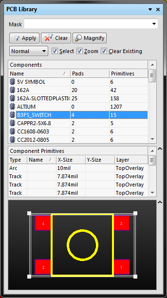
Right-click on the component in the PCB Library editor to place it, or to update an already-placed component.
Non-Graphical Editing...
The following methods of non-graphical editing are available:
...via an Associated Properties Dialog
This method of editing uses the following dialog to modify the properties of a Component object.
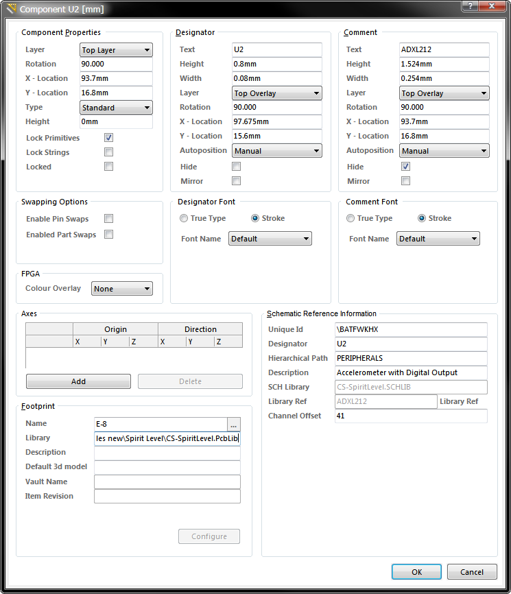
Edit the properties of the component in the dialog.
The Component dialog can be accessed prior to entering placement mode, from the PCB Editor – Defaults page of the Preferences dialog. This allows the default properties for the component object to be changed, which will be applied when placing subsequent components.
During placement, the dialog can be accessed by pressing the Tab key.
After placement, the dialog can be accessed in one of the following ways:
- Double-clicking on the placed component object.
- Placing the cursor over the component object, right-clicking and choosing Properties from the context menu.
...via an Inspector Panel
An Inspector panel enables the designer to interrogate and edit the properties of one or more design objects in the active document. Used in conjunction with appropriate filtering, the panel can be used to make changes to multiple objects of the same kind, from one convenient location.
...via a List Panel
A List panel allows the designer to display design objects from one or more documents in tabular format, enabling quick inspection and modification of object attributes. Used in conjunction with appropriate filtering, it enables the display of just those objects falling under the scope of the active filter – allowing the designer to target and edit multiple design objects with greater accuracy and efficiency.
Graphical Editing
Graphical component editing is limited to moving, rotating and flipping. When a component is selected in the workspace it is highlighted in the current selection color, as shown in the image below. To graphically manipulate a selected component:
- Press Delete to remove the selected component from the design.
- Click and hold to move the selected component, the cursor will jump to the component reference point, or the nearest pad center if the Smart Component Snap option is enabled (PCB Editor - General page of the Preferences dialog)
- While a component is moving on the cursor press the Spacebar to rotate it (Shift+Spacebar to rotate in the other direction).
- While a component is moving on the cursor press the L key to flip it to the other side of the board.
Click once to select a Component or click and hold to move it. Press the Spacebar to rotate while moving.