Bending Line
Parent page: Objects
Summary
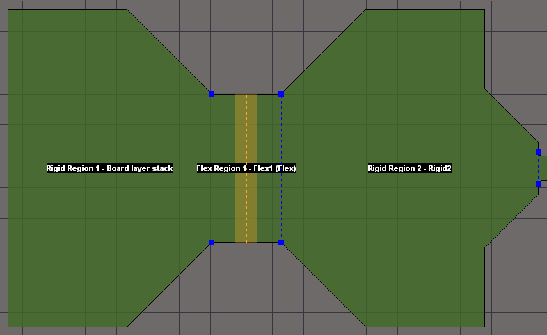
A Bending Line is a drawn PCB object that defines how a flexible board should be bent. Bending Lines can be placed across a Board Region that has been assigned a Layer Stack with the Flex option enabled – that is, the particular board region has been configured as flexible.
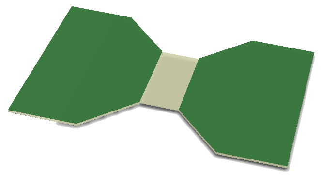
A Bending Line defines where on the surface of the flex region the bend is to take place. It also defines the angle and radius of the bend, and the width of the strip of board surface that is being bent. When the PCB editor is in 3D Layout mode the bends can be displayed in their progressively folded state, providing a real-wold look at the rigid-flex design.

Availability
Bending Lines are available in the PCB Editor when the View mode set to Board Planning Mode (View » Board Planning Mode – press the 1 shortcut).
Bending Lines can only be placed on a Board Region that has been assigned a Flex-configured layer stack. They are placed using Design » Define Bend Line from the main menu, or by using the the D, E shortcut keys.
Placement
To place a Bending Line:
- Select View » Board Planning Mode (or press the 1 shortcut) to enter Board Planning Mode.
- Select the Design » Define Bending Line command, or use the D, E shortcut.
- Click inside the board region where the Bending Line is to be placed, one end of the line will attach to the edge of the region closest to the click location, the other end will attach to the cursor.
- Position the second end in the required location then click once to place it.
- You remain in Bending Line placement mode, ready to place another Bending Line if required. If not, right-click or press Esc to exit Bending Line placement mode.
Non-Graphical Editing...
The following methods of non-graphical editing are available:
...via the PCB Panel
The PCB panel allows you to browse the current PCB design using various filter modes to determine which object types or design elements are listed, highlighted or selected. It also has editing modes for certain object types or design elements that provide you with specific controls on the panel for editing procedures. Board regions, Split Lines and Bending Lines are available for examination and editing when the PCB editor is in Board Planning Mode (press 1).
Set the PCB panel browsing mode (top drop-down list) to Layer Stack Regions. The panel shows:
- The available board layer stacks, in the Layer Stacks list area.
- The Regions assigned to those stacks, in the Stackup Regions list area.
- The Bending Lines defined in the selected Region, in the Bending Lines list area.
To edit the properties of a Bending Line:
- Select the Board Region that contains the Bending Line in the Stackup Regions area in the PCB panel.
- Select the Bending Line from the list in the panel's Bending Lines list area. The bend line will be highlighted (selected) on the board if the PCB panel's Select option is enabled. A Bending Line entry can also be deleted from the Bending Lines List.
- Double-click on the Bending Line entry in the Bending Line list (or the bend line itself on the board) to open the Bending Line properties dialog.
- Edit the Bending Line properties in the Bending Line dialog as detailed below.
Note that Bending Line dialog can also be opened by pressing Tab while placing or moving a bending line node (end-point handle).
...via the Associated Properties Dialog
A Bending Line's properties can be accessed and edited from the Board Region dialog, which is opened by double-clicking on a selected Bending Line entry (see above). Note that the PCB editor should be in the Board Planning Mode view – View » Board Planning Mode [shortcut 1].

In the Bending Line dialog, edit two of the first three properties, for example the Radius and the Bending Angle. The third property (area width) will be calculated automatically. Note that each Bending Line's Affected area width is displayed on the board in dark yellow.
The Fold Index defines the sequence that the bends are folded when the Fold State slider or View » Fold/Unfold command is used. The slider is in the PCB panel, just below the Bending Lines section – use it to fold the board up in 3D mode.
Click OK to accept the new setting and close the dialog.
Graphical Editing
A Bending Line can be graphically edited by manipulating the nodes (vertexes) at the end of each line using a select and drag method.
To move a Bend Line:
- Select View » Board Planning Mode (or press the 1 shortcut) to enter Board Planning Mode.
- Click to selected the Board Region that contains the Bending Line.
- To relocate the end of a line, click, hold and drag the node to the required location on the perimeter of the board region outline. The cursor will be constrained to the current snap grid and/or existing design objects.
- The bend location will be redefined by the Bending Line's new position.
To remove a Bending Line:
- Select View » Board Planning Mode (or press the 1 shortcut) to enter Board Planning Mode.
- Click and hold one of its end points, then press the Delete key. Alternatively, select and delete a bend line entry in the PCB dialog's Bending Lines list.