Add Shielding to Net
Parent page: PCB Dialogs
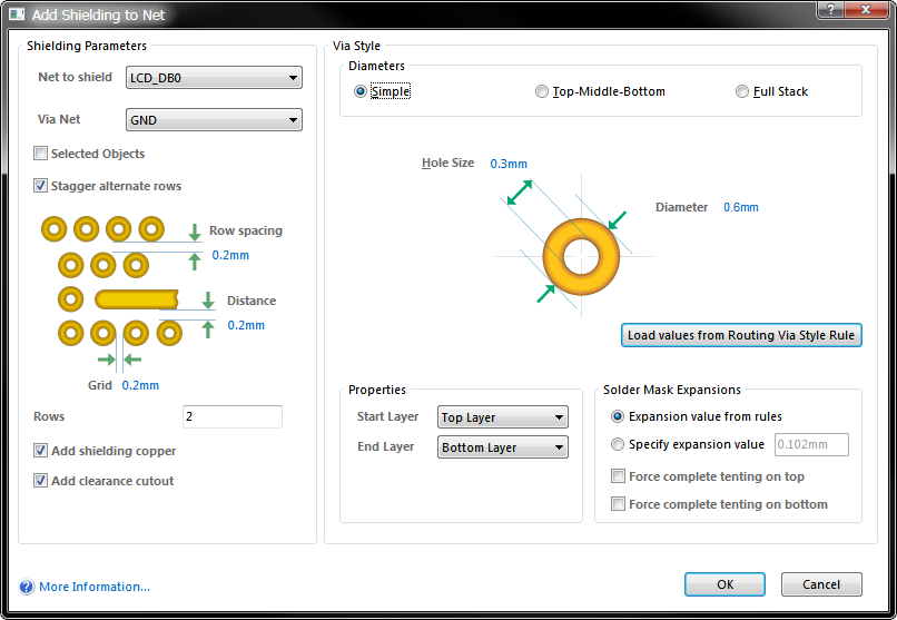
The Add Shielding to Net dialog.
Summary
A via shield is used to create a vertical copper barrier through the PCB, to help reduce crosstalk and electromagnetic interference in a route that is carrying an RF signal. A via shield, also known as a via fence or a picket fence, is created by placing one or more rows of vias alongside a signal route.
Access
In the PCB Editor, run the command Tools » Via Stitching/Shielding » Add Shielding to Net.
Options/Controls
Shielding Parameters
The shielding parameters control the shielding vias' placement pattern, and their clearance from other-net and same-net objects.
- Net to shield - net to have shielding vias placed around.
- Via Net - net that the shielding vias are to connect to.
- Selected Objects - place shielding vias around the selected objects, rather than the entire net selected in the Net to shield field.
- Stagger alternate rows - alternate rows of shielding vias are offset by half of the Grid value.
- Row Spacing - spacing between rows of shielding vias (edge to edge separation), when Rows setting is greater than 1.
- Distance - separation from the edge of the shielded net track segments, to the edge of the shielding vias.
- Grid - the distance between the edges of adjacent shielding vias. Shielding vias will not be placed in violation of applicable design rules, if a potential via site would result in a violation then that site is skipped.
- Rows - number of rows of shielding vias.
- Add shielding copper - place a polygon over the area occupied by the shielding vias, connected to the net specified in the Via Net field. The polygon is defined in accordance with the applicable Clearance constraint and Polygon Connect Style design rules.
- Add clearance cutout - include a polygon cutout around the shielded net, set back from the net by the distance specified in the Distance field. Use this when you require a different clearance from the applicable Clearance constraint design rule.
Via Style
The shielding Via Style can be configured manually in the Add shielding to Net dialog, or imported from the applicable Routing Via Style design rule by clicking the Load values from Routing Via Style Rule button. Clicking this button will load the Preferred rule settings.
Diameters
- Simple - Via Style(Hole size and diameter) is the same through all layers.
- Hole size - Specify the hole size value for the Via.
- Diameter - Specify the diameter for the Via.
- Top-Middle-Bottom - Different Hole Size and Diameters can be set at Top Layer, Middle Layer and Bottom Layer respectively.
- Hole size - Specify the hole size value for the Via.
- Top Layer - Specify via size for top layer.
- Middle Layer - Specify via size for Middle layer.
- Bottom Layer - Specify via size for Bottom layer.
- Full Stack - Different Hole Size and Diameters can be edited at each layer(including all signal layers and planes).
- Hole size - Specify the hole size value for the Via.
- Edit Full Stack Via Sizes - Click to open Via Layer Editor dialog, in which to specify via settings for each layer stack.
Properties
- Start Layer - Specify the start layer of the via.
- End Layer - Specify the end layer of the via.
Solder Mask Expansions
- Expansion value from rules - Enable this option to allow the existing solder mask expansion rule to take effect on this pad object. Check the Mask design category from the PCB Rules and Constraints Editor dialog.
- Specify expansion value - Enable this Specify expansion value option to edit the expansion value and the solder mask expansion design rule is overridden for this pad.
-
Force complete tenting on top - Enable the Force complete tenting on top option and any solder mask settings in the solder mask expansion design rules will be overridden and results in no opening in the solder mask on top layer of this pad.
Disable this option and this pad is affected by a solder mask expansion rule or specific expansion value. -
Force complete tenting on bottom - Enable the Force complete tenting on bottom option and any solder mask settings in the solder mask expansion design rules will be overridden and results in no opening in the solder mask on the bottom layer of this pad.
Disable this option and this pad is affected by a solder mask expansion rule or specific expansion value.
Notes
- Each set of shielding vias are added to a union. The set can be removed by running the Tools » Via Stitching/Shielding » Remove Via Shielding Group command, then clicking on any via in the group.