Panelization using the Embedded Board Array Feature
In the board design world there is actually 2 distinctly different uses of the word routing. There's the routing of the nets across and through the board to connect the various nodes in the net. Then there's the routing, or milling, process that is used to cut slots and holes in and around the board, often to help remove each board from the fabrication panel. The milling-type of routing can be spelt as route, or rout.
Almost all boards are panelized for fabrication - fabricators use standard sized panels in their processes so multiple images of the board are placed to most efficiently use the area available on that panel. Panels can also be created as a mixture of different boards, as long as they all share the same set and arrangement (stackup) of copper layers. These panels are often used through the assembly process as well.
Altium Designer has excellent support for creating panels, using the embedded board array feature. Rather than embedding the actual board into the panel, it is done using a link back to the original board file(s) - making it easy to update the actual individual board(s) and refresh the panel. This approach also allows the designer to panelize different boards onto the same panel. If any of the linked, individual boards changes, it is simply a matter of refreshing the embedded board array to update it with the latest linked-board data.
There are 2 main techniques used to ensure that the individual boards can be removed from a panel, they are scored around each edge to define snap lines, or slots and holes are routed and drilled around the edges to free each board, or a mixture of both techniques are used.
Visualization of the Rout Tool Path
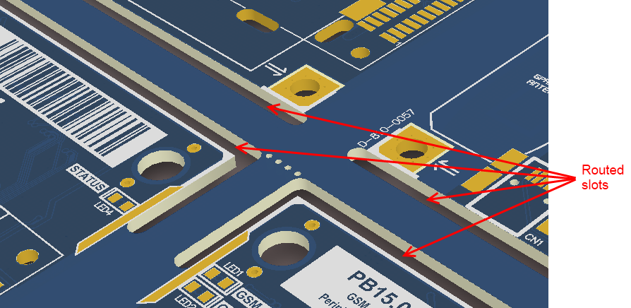
Rout paths are typically defined by placing track (line) objects on a mechanical layer. The width of the track defines the diameter of the rout tool, and the X, Y coordinates define the rout cutting path. To examine what the routed slots will look like, select the mechanical layer that has been used to define the routing in the Route Tool Path option of the Board Options dialog, then switch the board display to the 3D mode (press the 3 shortcut).

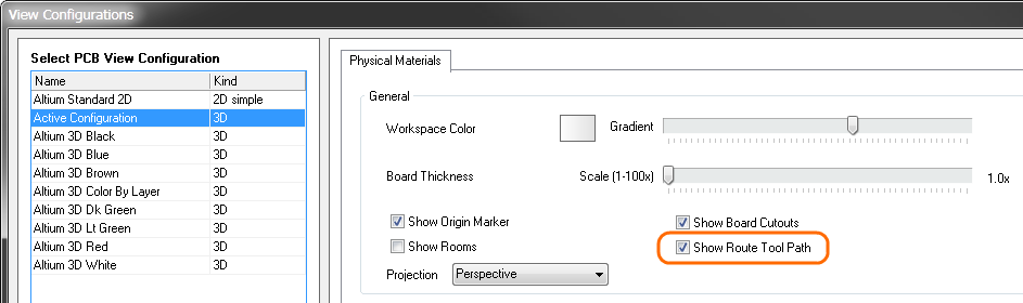
After switching the display of the board to 3D mode, open the View Configurations dialog (press the L shortcut), and enable the Show Route Tool Path option, as shown below.
When the board is displayed in 3D mode, track and arc objects detected on the Route Tool Path layer will be displayed as slots in the board. A common approach for passing this information to the board fabricator is to generate Gerber data of this mechanical layer, and then advise the fabricator that this layer is actually routing data. They will convert that Gerber file into the format required by their milling machine.