Configuring the Grids, Layers and Colors
PCB Layers and Colors
The PCB Editor is a layered design environment. It is these layers that create the 3rd, or Z-dimension of the 3 dimensional board structure, and you create the board design by placing objects on these layers.
These layers are either:
- physical layers, from which the PCB fabrication information is created;
- mechanical layers, used for notes and other documentation detail; or
- system layers, such as the grids and hole display layers.
Physical layers include the signal layers, internal plane layers, silkscreen, solder mask and paste mask layers. Each of the layers is assigned an identifying color, to help you as the designer understand and interpret the design content.
Apart from pads and vias, objects are placed on a specific layer, this layer is made active by selecting its Tab at the bottom of the workspace, before placement.
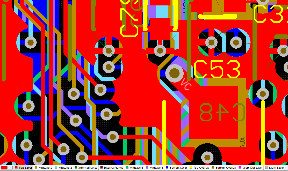
The many layers in a PCB design make it a dense and busy workspace, in this example the Top Layer is the active, or current layer, as shown by its Layer Tab.
Physical layers are added and configured in the Layer Stack Manager. As well as the signal and plane layers, the layer stack also includes the non-electrical, dielectric layers. These are included to allow accurate definition of the board in the Z-plane, and are essential for correct calculation of route lengths and signal integrity properties, such as route-path impedances.
Mechanical and system layers are added and configured in the View Configurations dialog. The visibility and color of each layer is configured here. Default layer colors are defined in the PCB Editor — Layer Colors page of the Preferences dialog. Colors are loaded from a color profile, and user-defined profiles can also be created and saved.
The Unified Cursor Snap System
Main article: Unified Cursor-Snap System (PCB)
The PCB Editor is a grid-based design environment, design objects are placed on what is referred to as the placement, or snap grid. As well as the placement grid, Altium Designer includes a number of snap features, designed to help you accurately position and align design objects. Together, these features are referred to as the Unified Cursor Snap System.
Placement Grids
Main article: Grid Manager (PCB)
The PCB Editor is a grid-based design environment, design objects are placed on what is referred to as the placement, or snap grid. The current snap grid setting is always displayed on the Status bar at the bottom of Altium Designer, along with the cursor location, relative to the Current Origin.
![]()
The Status bar always displays the current snap grid and the cursor location, relative to the Current Origin.
The current origin is user-definable and can be located anywhere in the workspace, the Absolute Origin is the bottom left of the 100 x 100 inch workspace.
Any number of Cartesian or polar grids can be defined in the workspace, with only the highest priority available grid being active at any time. Grids are defined in the Grid Manager, as well as the grid setting, you also define the grid area, grid color, the multiplier for the Fine and Coarse grid lines, and choose Lines or Dots for the grid display.
Object Snap Points
Main article: Object Snap-Points
It is often impossible or impractical to define a grid that all design objects fall on to. In that situation you might need to position a new design object at an off-grid location. Altium Designer supports this through a feature called Object Snap, which is essentially a range of attraction around that object's hotspot. Hotspots only exist at meaningful locations, such as the center of a pad or via, and the end points of track segments. The range of attraction is defined in the Board Options dialog, when the cursor moves within this range of a hotspot, it automatically snaps to it. The animation below shows the object snap in action, the range has been set to a large value to make it easier to see the behavior.
The cursor changes to include a circular ring when it hits a hotspot. Note that the state of the Hotspot Snap is also detailed on the Status bar, as shown in the image above. Press the Shift+E shortcut to cycle the setting to On (current layer objects only), On (objects on all layers), or Off. Alternatively, press Ctrl during placement to temporarily inhibit it.

Off grid objects can be snapped to, using the object snap feature.
As well as snapping the cursor to an object's hotspot, Altium Designer also supports snapping to an object's axis, as shown in the animation below. This supports aligning the moving object to existing off-grid objects. The Snap to Object Axis behavior is also configured in the Board Options dialog, click Advanced to configure it.
Off-grid objects can be aligned, using the object axis snap feature.
Snap Guides and Snap Points
Main article: Snap Guide Manager (PCB)
As well as the object-to-object snap behavior described above, Altium Designer also supports user-definable Snap Points and Snap Guides. These are placed in the workspace via the Snap Guide Manager. Note that their location is changed by editing the X and Y settings in the dialog, or by clicking the ![]() button in the X or Y edit field to interactively select an X or Y location the workspace.
button in the X or Y edit field to interactively select an X or Y location the workspace.
Click the Snap menu to access all of the Unified Cursor Snap features.