Moving to Altium Designer from Mentor Graphics DxDesigner
Contents
- Getting Started - Transferring Your DxDesigner Designs
- Using the Import Wizard for DxDesigner Designs
- Schematic Design File Translation
- Schematic Design Object Translation
- Schematic Library File Translation
- Schematic Symbol Translation
- Using the Import Wizard for PADS Layout Files
- Layer Mapping for PADS PCB ASCII Files
- Working with Documents in Altium Designer
- The Schematic Symbol is the Part
- Design Rule Scoping
- Altium Designer Libraries
- See Also
Many DxDesigner® users use a combination of PADS Layout® for their PCB layout, and DxDesigner for their schematic capture. This application note assumes this combination.
Getting Started - Transferring Your DxDesigner Designs
Translating complete Mentor Graphics® DxDesigner® designs, including schematics and library files can all be directly imported by having Altium Designer's Import Wizard without having to convert to an intermediary format - thus avoiding the need for having DxDesigner installed. Such files will be converted into Altium Designer schematic documents (*.SchDoc) - one schematic document per sheet defined within the Logic file - and added to a PCB project (*.PrjPcb).
The Import Wizard (File » Import Wizard) removes much of the headache normally found with design translation by analyzing your files and offering many defaults and suggested settings such as project folders, project links to other libraries, drawing styles, and output project structure. Complete flexibility is found in all pages of the wizard, giving you as little or as much control as you would like over the translation settings before committing to the actual translation process.
Using the Import Wizard for DxDesigner Designs
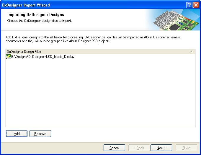
You can drag and drop your designs directly from Windows Explorer project folders into the designs and libraries page of the Import Wizard.
You can use the Import Wizard whether using DxDesigner schematic files by themselves or in combination with a PADS Layout PCB. Because there is a difference in the way that project files and schematic files are named and organized between DxDesigner and Altium Designer, it's worth briefly reviewing this so that you understand exactly how your schematic design and libraries files will be translated after the import process.
DxDesigner manages the design project based on a user-defined directory path, and everything in the system uses this project path as the initial point of reference. For example, instead of using file extensions for a file's type, a folder called sch in the project path indicates that files under this folder are schematic files. The individual schematic files follow the naming convention of Name.N where N is a numeric number. An example of this would be schematic_design.1. DxDesigner identifies this as a schematic file only because it is in the specified project path and under the folder called sch. Likewise, a folder called sym in this project path indicates it is a symbol folder, and that all files under it are assumed to be the equivalent library files (also following the same naming convention as schematic files).
Altium Designer uses specific file extensions for certain file types such as schematic design files, library files and project files. As you begin to import your DxDesigner files using the Import Wizard, you will be asked for your project directory name. The Import Wizard knows to look for the sch and sym folders inside the specified project path. If that directory does not exist, you will be given a warning message.
Schematic Design File Translation
DxDesigner project paths and schematic files in the Import Wizard translate as follows:
Project paths have an equivalent Altium Designer PCB (*.PrjPCB) project automatically created for them. Once translated, files are grouped into that PCB project. For example, if you specified C:\my_projects\LED_Matrix_Display as the DxDesigner project path, the Import Wizard will create LED_Matrix_Display.PcbPrj in Altium Designer.
Schematic files (Name.N) translate to Altium Designer schematic files (*.SchDoc). Each schematic file will be imported as a single Altium Designer schematic file. Design hierarchy is maintained, including complex hierarchy.

Translated design files are displayed immediately after translation in the Projects panel. Once the project has been compiled the schematic hierarchy will be shown.
Schematic Design Object Translation
Most component attributes are translated into parameters with a few exceptions:
Power Objects - DxDesigner symbols that contain a NETNAME attribute are identified as and translated into power objects in Altium Designer.
Ports - Similar to power objects, a symbol with an attached attribute represents it as a port. DxDesigner symbols that contain an IN, OUT, or BI attribute are identified and translated into Input, Output, or Bidirectional ports respectively.
Signal - Symbols that contain a SIGNAL attribute are identified as and translated into hidden power pins.
Reference Designator - The REFDES attribute attached in the DxDesigner symbol usually has the format of: REFDES = R? When it is placed into a sheet, the user will specify the REFDES of the component in the sheet i.e. REFDES = R21.
Other common design objects translate as follows:
DxDesigner wire segments and busses translate to wires and busses respectively.
A wire or bus segment in DxDesigner can have a label attached to it. This is translated into a net label. Net label strings in DxDesigner with the following format D [0:8] are replaced with the following format D [0..8].
Composite symbol types are identified and translated as Altium Designer sheet symbols. The symbol pin is translated as sheet entries and the sheet symbol file name will point to the list of schematic sheets that matches the symbol file prefix.
Schematic Library File Translation
DxDesigner symbol library files translate as follows: symbol files (Name.N) translate to Altium Designer library files (*.SchLib). Each symbol file will be imported into a single Altium Designer library file. Once translated, files are grouped into the Altium Designer PCB project (*.PrjPCB) that is automatically created.
Schematic Symbol Translation
Component Name - the following table describe how the DxDesigner symbol translates to the Altium Designer component:
| DxDesigner Symbol | Altium Designer Component |
|---|---|
| Symbol file name. | Component name |
| REFDES attribute | Designator |
| Use from the DEVICE attribute | Comment |
| Any other symbol attribute | Parameters |
Pin Type - the following table maps the PINTYPE attribute from DXDesigner to Altium Designer:
| DxDesigner Pin Type Attribute Value | Altium Designer Pin Type |
|---|---|
| BI | IO |
| TRI | HiZ |
| ANALOG | Passive |
| OCL | Open Collector |
| OEM | Open Emitter |
Graphical Objects - Most objects have a direct translation from DXDesigner to Altium Designer. Boxes (as defined as lower left and upper right corners) translate to four-point polygons.
Multiple-part symbols - The PARTS attribute attached to the symbol indicates the number of parts this symbol represents and translates to the number sub-parts in Altium Designer.
Annotate Symbol Type - DxDesigner categorizes the symbol into four types: composite, pin, annotate, and module. The most common use of symbols in DxDesigner is for sheet borders and graphical annotation. Because of this reason, such symbols are translated in Altium Designer components with a TYPE = Graphical.
Heterogeneous Symbols - Heterogeneous symbols in DxDesigner are any group of symbols that have the same HETERO attribute. When symbols are grouped under one HETERO type, they represent one device. Altium Designer translates these symbols to multiple parts or display modes under one component depending on the heterogeneous type. There are three distinct types:
- HETERO TYPE 1- Different components within the same device. The Altium Designer attribute assigned to this type follows the format: HETERO = sym1, sym2, [sym3].
- HETERO TYPE 2 - Different gates within the same device. The Altium Designer attribute assigned to this type follows the format: HETERO = sym, (symP) where P = PARTS number.
- HETERO TYPE 3 - This is a split IC. The Altium Designer attribute assigned to this type follows the format: HETERO = (icsymname), (icsymname). The main difference between this type and HETERO TYPE 1 is only the context used by DxDesigner related to ICs.
Using the Import Wizard for PADS Layout Files
The Import Wizard can be launched from the Altium Designer File menu. Click on this menu command to invoke the wizard. Right-click command menus are available for further control over the translation process through each page of the wizard.
Files in the Import Wizard translate as follows:
- PADS ASCII PCB Layout (*.ASC) files translate to Altium Designer PCB files (*.PcbDoc).
- PADS ASCII PCB Library files translate as follows translate into Altium Designer PCB library files (*.PcbLib).
- These files will be grouped into an Altium Designer PCB project (*.PrjPCB) that is automatically created.
Layer Mapping for PADS PCB ASCII Files
All used PADS PCB layers must be mapped to an Altium Designer layer prior to import when using the Import Wizard. There are additional options provided to control the automatic creation of design rules, missing vias and keep-out conversions as well.
Use the Layer Mapping Options from the Edit Mapping button in the Import Wizard to associate PADS PCB layers to Altium Designer layers.
It should be noted about how the layers are mapped on import for PCB designs. Layer Mapping is simply a mapping between the names of the PADS PCB layers and Altium Designer PCB layers. Of course you can change as many mappings as you want as only suggested default mappings are given. This mapping is used by the Import Wizard to build the layer mapping for each PCB that can then be individually customized. The rationale here is that should you wish to import ten PCB designs and you want to map the layer Assembly 1 to Mechanical Layer 1, you would not have to customize each of the ten PCB designs in order to get the right layer mapping.
The advantage to importing in this manner is that batch management of layer mapping can save a lot of time when importing multiple designs. In this instance, the default layer mapping will be saved to your Preferences. The disadvantage to using this is that Default Layer Mapping is not always intelligent with differing structures in designs, and so some manual changes may be needed afterwards. You'll need to decide what is best for your situation.
Working with Documents in Altium Designer
In PADS Layout all design work begins on the workspace, the logical working area of the PCB design. Each design is saved to a single design file (*.PCB file). There are also physical design reuse files (*.REU) which allow you to preserve a portion or subset of a PCB design for reuse within the design or in another design - these are ignored and not translated.
In Altium Designer, the logical design area begins with a document, and for each document there is a file stored on the hard drive. This means that for each Altium Designer schematic sheet (page) there is a file, an important conceptual difference to remember.
There can also be multiple design documents of varying types, depending on the nature of the design you are working on. Getting started, most DXDesigner users will be interested in the schematic and PCB document types as these are the files that their designs will be translated to.
Basic file operations: new PCB and schematic document types can be easily created via File»New, or by right-clicking on the project in the Projects panel.
The Schematic Symbol is the Part
As an expert PADS Layout user, you'll know that parts form the basic building blocks of design in PADS Layout. Parts are defined as having a part type, a logic family, number of pins, number of gates, and signal pins. The term component is only used when the part becomes placed as a physical object in the PCB layout design.
In PADS Layout (PCB), a part can represent one or more physical components. Parts in PCB designs usually correspond to physical objects: gates, chips, connectors, objects that come in packages of one of more parts. Multiple-part packages are physical objects that are comprised of one or more parts.
In DxDesigner, a symbol block type is the logical entity that is described graphically by attributes, pins and various properties. As block types are placed in a schematic design, DxDesigner maintains the identity of the part for back annotation, net listing, bills of materials, and so forth. At the very minimum, a part requires a part name, a part reference prefix, and a name of a PCB footprint.
These two definitions that use the same term depending on the context of design may initially cause some confusion in the new environment which uses the term component. But it is not unlike how things work in Altium Designer except that the schematic symbol is effectively the part for all phases of design, and not just the PCB Layout portion of it.
In Altium Designer, the logical symbol is assumed to be the essential starting point of a component. It can be initially defined at minimum as a name in a schematic library to which pins and any graphical symbols or alternative display options needed for implementation may be added. This flexibility allows a component to be represented in different ways during the design and capture process. This may not only be as a logical symbol on the schematic, but also be a footprint on the PCB or even as a SPICE definition for simulation.
Design Rule Scoping
Main article: Design Rules
Rules Scope - the extent of a rule's application - replaces the Rules Hierarchy from PADS Layout. A scope is effectively a query that you build to define all the member objects that are governed by that rule, giving you full control. For the sake of a baseline comparison, let's review the Rules Hierarchy of PADS Layout. These rules rely on a pre-defined list format where higher numbers on the list have precedence over those that are lower:
- Default
- Class
- Net
- Group
- Pin Pair
- Decal/Component
In the PADS Layout rules schema, Default rules are considered level 1 and are the lowest while Decal and Component rules represent the highest. Conditional layer rules can be applied for an additional level of precedence. For example, a Default with a conditional layer rule would be higher in the precedence hierarchy than a simple Default rule.
In Altium Designer, scoping allows you to decide exactly what a rule's precedence will be and how it will be applied to target objects through a query. You can even define multiple rules of the same type, but each targeting different objects. Queries are easily accessed for any rule (Figure 22). Advanced (Query) options are also available to help you write your own, more complex queries.
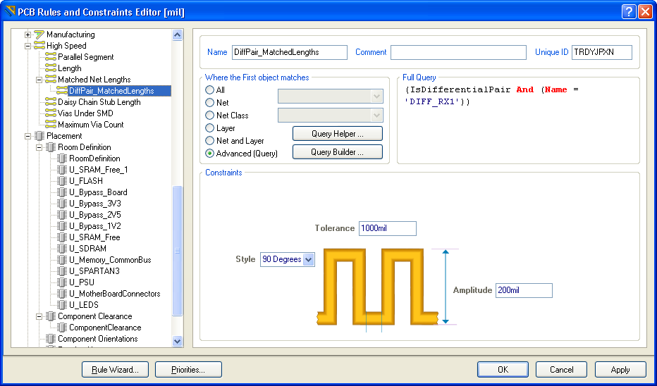
Double-clicking on any rule while in the PCB Rules and Constraint Editor dialog will bring up the specific query for that rule in the right panel.
If you do not want to use a design rule, but may want to use it in the future, rather than delete it you can simple disable it. Toggle the corresponding Enable option for the rule in the relevant list.
All default design rules have a scope (Full Query) of ALL, meaning that they apply to the whole board. In addition to scoping, there is also a user-defined priority setting. The combination of rule scoping and priority is very powerful and gives an unprecedented level of control that allows you to precisely target the design rules for your board.
Altium Designer Libraries
An integrated library in Altium Designer is one where the source symbol, footprint, and all other information (e.g. SPICE and other model files) are compiled into a single file. During compilation checks are made to see how relationships are defined, to validate the relationship between the models and the symbols and to bundle them into a single integrated library. This file can not be directly edited after compilation, offering portability and security.
All of Altium Designer's 70,000+ components are supplied in integrated libraries, from which the source libraries can be extracted at any time if required.
| PADS Object | Altium Designer Object | Comments |
|---|---|---|
| Decal | Footprint | Graphical representation of the shape defined for the component to mount onto the PCB. This is 2-dimensional representation only, and can be quite different from the actual component itself |
| Part | Part/Component | The term Part is used only as part of the design capture (schematic) process in Altium Designer. Once placed as a footprint into a PCB file, it is given a designator and value (comment) |
| Lines | Lines | Primitive object used for graphical information. |
| CAE Decal | Schematic symbol | The graphical representation of a schematic part, such as a NOR gate. |
A table of the more commonly-used PADS Library terms and their closest respective Altium Designer equivalents.
See Also
Below are references to other articles and tutorials in the Altium Wiki that talk more about the conceptual information, as well as walking you through specific tasks. Remember, you can also browse through the Help contents, and use F1 and What's This at any time in a dialog for more details.
For more PCB project options, refer to the tutorial, Getting Started with PCB Design.
For more FPGA project options, refer to the tutorial, Tutorial - Getting Started with FPGA Design.
For a tutorial that steps you through all the basics of creating components, read Creating Library Components Tutorial.
For a tutorial that steps you through all the basics of editing multiple objects, read Editing Multiple Objects.
For an overview of Altium Designer's FPGA design, development and debugging capabilities, read Soft Design.