Board Implementation - FAQs
Board Implementation - FAQs
Use the following links to browse through frequently asked questions about board implementation in Altium Designer.
How do I include a graphic on the PCB design?
Here are 2 ways of getting a graphic onto your PCB design.
Pasting from the Windows Clipboard
The PCB editor supports pasting a metafile directly from the Windows clipboard, into the current PCB layer, using the standard Windows CTRL+V Paste command. Note that not all image editors place the image data into the clipboard as metafile data, one approach to ensure that this happens is to first paste the image into Microsoft Word, then copy it from there and paste it into Altium Designer.
Supported metafile data includes bitmaps, lines, arcs, simple fills, and true type text - allowing you to easily paste logos and other graphical symbols. Imported data will be put onto the current layer, adopting the color you have chosen for that layer. The PCB objects created during the paste process are automatically added to a Union. After pasting, use the Union resize handles can be used to fine-tune the size of the paste image. Unions resulting from a paste can also be resized at any time using the Resize Union command from the right-mouse menu (click to select the required union after launching the command).
The Paste from other applications option in the PCB Editor — General page of the Preferences dialog is used to set the Preferred Format to Metafile or Text. For a graphic this option has no impact, each independent shape in the graphic is converted to a region object. When pasting a text string, each character is converted to a text string if the option is set to Metafile, whereas the entire string is pasted as an Altium Designer string if the option is set to Text.

The Altium logo being pasted as a graphic, each letter in the graphic is converted into a region object
Placing a Graphic as a Font
It is possible to create a custom TrueType font that contains a graphic as a glyph (one of the characters in the font) and then place a string on the PCB board that uses that font. As well as the ease of use, another great advantage of this method is that if the font glyphs are created from vector graphic images, then they can be accurately scaled.
A font of many standard symbols used in PCB design, including: lead free, recycle, static sensitive, Earth, C-Tick, UL, CE, FCC, and many others, has been created by one of the leading experts in designing in Altium Designer, Darren Moore from Mooretronics. The font is available for download here (dated June 2015), and you can also check the Altium Designer forum thread, for more recent versions in the latest posts.
The font is licensed as Cardware, refer to the Readme.txt included in the download ZIP for conditions of use. The readme also includes a list of the available graphics. Note that many are available with text or without text, the preferred version is chosen by using the upper or lower case letter. The image below shows a sample of the graphics available in the font.
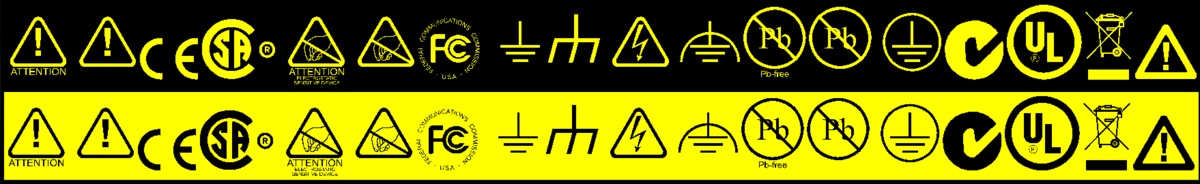
A sample of some of the useful graphics in the Mooretronics font.
Why is my polygon clearance rule ignored?
The most common reason for a polygon clearance rule to fail is that it is targetting the polygon as a single entity, rather than the rule targetting the primitives that make up the polygon. To target the primitives within the polygon, Clearance rules for polygons must use the InPolygon, InPoly or InNamedPolygon keyword, as opposed to IsPolygon.
Polygon Pours should be thought of as containers for either Region or Track objects, which are regenerated as needed when the polygon pour is repoured. The tracks and regions constitute the physical copper that is created in the PCB manufacturing process. Other objects that correspond to physical copper are arcs, fills, strings, pads and vias. The clearance rule will only operate these so called 'copper objects'. A clearance rule query will not work if it targets Polygon Pour objects, for example if the query IsPolygon is used. The query needs to target the regions or tracks that are part of the polygon pour, for example InPolygon.
Another thing is to ensure is that Polygon clearance rules have a higher priority than the general clearance rule (between All and All). 1 is the highest priority.
Examples:
Set the Clearance between Polygon Pour's and all other objects
| First Query | InPolygon |
| Second Query | All |
Set the Clearance between Polygon Pour's attached to nets in the net class 'Power', and all other objects
| First Query | InPolygon and InNetClass('Power') |
| Second Query | All |
Set the Clearance between Polygon Pour's and objects on the Top Layer
| First Query | InPolygon |
| Second Query | OnTopLayer |
Set the Clearance between a Polygon Pour named 'PolyPower_VCC_1' and vias in the GND net.
| First Query | InNamedPolygon('PolyPower_VCC_1') |
| Second Query | InNet('GND') And IsVia |
How do I navigate the board in 3D layout mode?
All 3D navigation is performed by clicking and holding on the right mouse button. RMB on its own to pan, add Ctrl to zoom, or add Shift to rotate.
The main tool used for navigation in 3D layout mode is the rotational sphere, as shown below. Hold Shift down to display the rotational sphere, it will appear at the current cursor location. Then while holding the Shift button down, right-mouse click to engage one of the modes of motion. The selected mode of motion is determined by which of the motion selectors is highlighted when you right-clicked, in the image below you can see that the center dot is highlighted, meaning that as you move the mouse around, the board will rotate around the sphere in all directions, tracking the motion of the mouse. The other modes of motion are flat rotation, X-rotation, and Y-axis rotation. Position the cursor over the required motion selector before you right-click, to select that mode.
Shift+right-mouse click and hold to rotate the board around the rotational sphere.
How do I add a snap point in the middle of a circle or object in a STEP model?
The reference points available in an imported STEP model may not be a suitable handle to use for positioning that object in Altium Designer. Typical reference points that a designer will want to use are the center of a hole, or the center of a pin.
The process of adding a snap point to the center of a circle (hole) or a pin is the same:
- Orient and zoom in on the model so the pin or hole is easily accessed.
- Select the Tools » 3D Body Placement » Add Snap Points from Vertices command.
- Keeping an eye on the Status bar, click once anywhere on the model to select the target STEP model.
- Now press the Spacebar, this toggles the command to its second mode, which is to define a Snap Point half way between 2 selected vertices (as detailed on the Status bar).
- Position the cursor to show the blue selection cross hair, locate it on one edge of the pin or hole, then click to choose that vertex.
- Position the blue selection cross hair on the second vertex, on the opposite side of the pin or hole, then click to choose that vertex.
- A Snap Point will be shown in the center of the pin or hole, as demonstrated in the animation shown below.
A Snap Point being added between the 2 chosen vertices.