利用嵌入式元件设计
传统的电路板设计是在板卡上下表面置元件,电路板组装车间完美支持该进程,在那里典型地应用自动拾取与放置机器来定位放置每个元件,并 准备好焊装在板卡表面。然而,随着更高集成度、更高信号速率、更小电子产品需求的刺激,驱使研究更好的制造安装电路板的方法。
有一个方法既可以实现高密度也可以满足高频信号的传输,那就是在电路板结构的板层中间嵌入元件。比如,在一个集成电路底下嵌入一个分立 的元件可以满 足:更短的信号长度,减少阻抗和寄生感抗,可以引起更低的电源噪声和EMI,而且可以获得更好的电路信号完整性。这些改进可以帮助设计更小更可靠的产品, 支持更快的信号速度更宽的信号带宽。同时,随着制造进程和技术的持续改进,他们还可以减小产品尺寸,减少制造和板卡组装的成本。
嵌入元件需要一系列非常规的命令用到每个设计阶段:从设计到制造,到组装,到测试,最后到完毕的产品。
如何嵌入一个元件?
嵌入元件介绍了制造电路板的一个重大变化——不再是简单制造一个裸板然后在组装过程中往裸板上装器件。这两项工作通常都由两个不同的公 司完成,因为 二者让人清晰地明白他们需要不同的进程以及不同的技术。如果使用嵌入式元件,必须在板卡制造过程中就得装好这些特殊器件。这是个高度专业化的领域,现在这 个制造过程已被许多生产厂家所掌握。
嵌入一个元件有两种方法:创建一个敞开的凹腔,以便嵌入式元件可以放置到凹腔中,成板上可以直接看到该凹腔;或者嵌入式元件可以在板卡 制造过程中放置到板卡内层中,然后盖上另一层封住,这样成板是看不到嵌入式元件的。
有许多处理方式来制造一个含有嵌入式元件的板卡,下面的描述和图片显示的是一种方式:
- 板卡起始于一个双层敷铜皮的硬板,铜皮按照要求蚀刻和钻孔;
- 半固化片+铜皮被放到每个层,同样按照要求蚀刻和钻孔;
- 嵌入式元件被安装在该层(单面或双面),利用比如焊膏沉积与回流处理;
- 执行一个半固化片层挖孔操作,每个挖孔为每个嵌入式元件创建一个凹腔;
- 一个半固化片+外层铜皮添加到上、底两边,仍然按要求蚀刻、钻孔并钻通孔(若有)。
板 卡使用累积技术制造,嵌入式元件被放置然后作为设计过程的一部分被包裹住。
记住,激光钻微孔通常用来到达板卡低位的嵌入式元件。
嵌入式元件设计
Altium Designer中,元件能被放置到任一信号层,而不像传统的放置在底层和顶层的表面。如果元件被放置在板内层的铜皮上且被覆盖住,那么这些元件被称之为 嵌入式元件。有两种方式嵌入元件:
- 一个用户自定义的凹腔建立起环绕元件所需的间距;
- 或者小封装型如0201,没有凹腔,则元件简单地由后续添加夹层到时候盖住,这会在成板上隆起一个包。
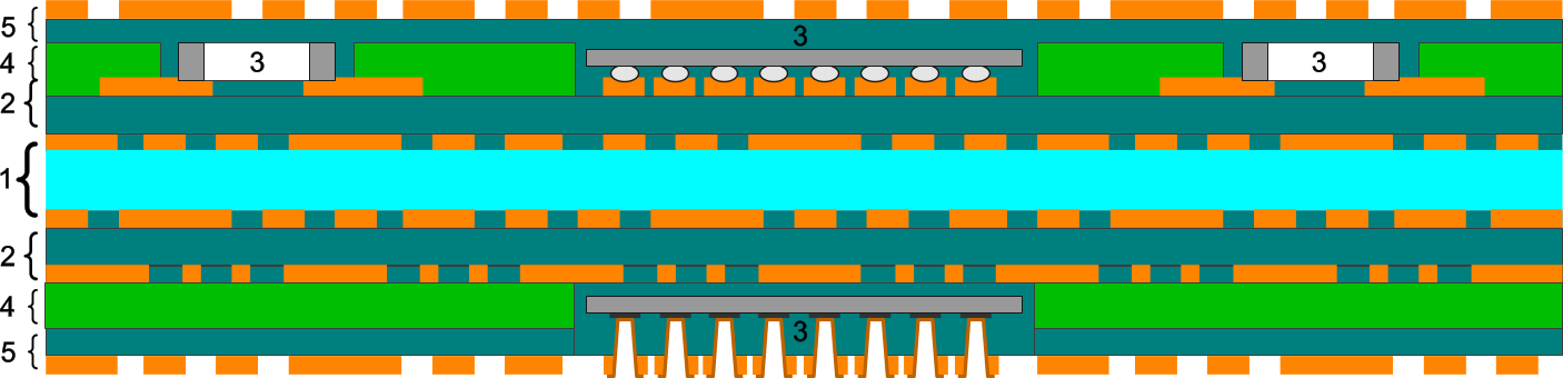
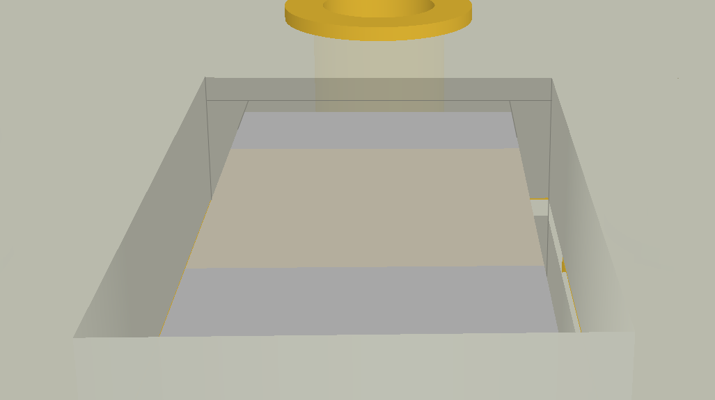
当一个元件需要一个凹腔,该凹腔可以最终被板卡封盖住,或者它能延伸到板卡的某一面形成一个敞开面。下图显示的是3个嵌入式元件,外面 的2个有一个 凹腔让它们敞开在板卡的顶层。中间的元件在一个较低位置的层上,这会让它被全覆盖住。从设计师的角度来看,元件放置的过程不管是开放式凹腔或者闭合的凹腔 都是一样的。
3 个嵌入式元件,2个外面的元件有个开放式的凹腔在板卡的表面,中间那个是彻底被嵌入板卡中的.
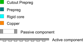
这 个元件被彻底嵌入。为了更好地解释这张图,元件用蓝色边框高亮,凹腔用橘色边框。
在PCB 库元件中定义凹腔
如果一个元件需要嵌入且它需要一个凹腔,那么凹腔在PCB 库编辑器中是作为封装的一部分的。记住,添加凹腔并不阻止元件在表面层的使用,这种情况下,软件将忽略该凹腔。
要定义一个凹腔:
- 在机械层放置一个Region对象。放置该对象以便将之装入该元件的3D体且有足够的边距。跟制造厂家确认需要多大的间距;
- 编 辑该Region对象并且设置Kind& nbsp;属性为Cavity definition;
- 确保Layer 属性是一个合适的机械层;
- 设置Height 属性为合适的高度,一般这都设置成跟3D体高度再加上制造厂家建议的间距。
下图显示的是PCB库编辑器,包含:
- 凹腔定义选择;
- 元件焊盘的红色轮廓;
- 3个紫色的阴影3D对象定义了电容的2个焊盘和元件主体。
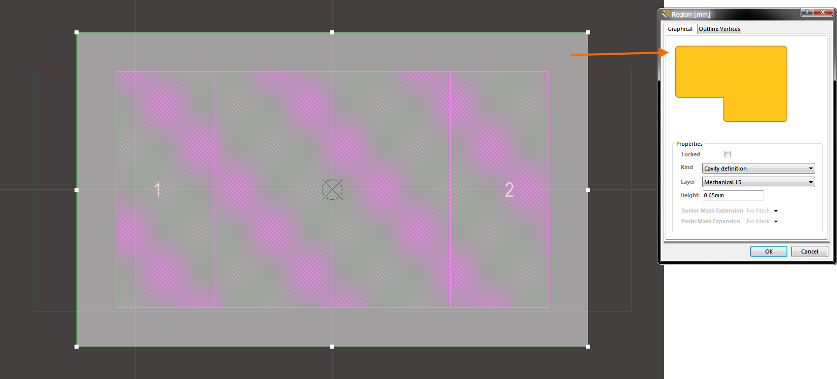
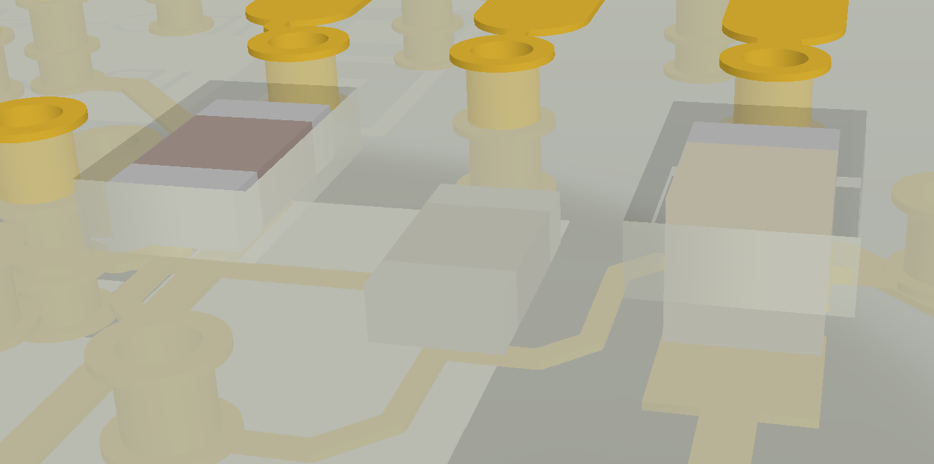
凹 腔通过在机械层上放置一个region对象然后设置其Kind属性为Cavity definition。注意紫色阴影区域,这是坐落在凹腔内的3D体。
放置并为嵌入式元件定方向
要嵌入一个元件,编辑该元件的属性,将Layer 设置到所需的内部铜皮层。嵌入式元件的方向(朝上是朝下)由Layer Stack Manager 对该层铜皮的Orientation 属性定义。如果需要,这个可以在元件的 属性对话框中使能Flipped on Layer复 选框来颠覆前面的方向定义。

在Component对 话框中设置元件的Layer, 如果需要,可以通过Flipped on layer覆 盖方向设置。
在Layer Stack Manager中 为每个信号层的元件设置Orientation。
设置凹腔高度
Related article: PCB Layer Stack Management
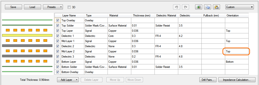
PCB库编辑器中定义的凹腔有一个Height属性。该高度属性定义了从元件所放置的层表面开始软件将移除所有层的高度距离。要简化凹 腔与它挖坑所 在各层之间的互动,软件会确保每层不会部分挖除。如果凹腔进入某层,比如一个电介质层,但没有延伸穿越全部该电介质层,那么软件将会自动延伸该凹腔到穿越 该层。下图显示的即是该情况:黑色所画线条显示了凹腔边角以及元件是如何坐落在挖空最后一层的表面下的。该行为既可以用在内层也可以在开放的凹腔。
如 果凹腔没有彻底穿越某层,则软件会自动创建彻底穿越该层的凹腔。
Embedded Components and Managed Stacks
When you embedded a component, Altium Designer has to manage how that embedded component affects the layer stack, not only in terms of how it is displayed, but also in terms of calculated data such as solder mask openings and design rule checking. It does this by creating a stack for each unique combination of placed + cut layers needed by the various embedded components included in the design. These stacks are referred to as Managed Stacks.
The Managed Stack is created automatically when a component is embedded within the layers of the board. As managed stacks are created automatically there is no user-input needed in their creation and management. Altium Designer checks for embedded components, tests if any of the current managed stacks are suitable and if not, creates a new one. The same applies when embedded components are removed, if a managed stack is no longer needed, it is automatically removed. To force Altium Designer to check if new managed stacks are needed, switch between 2D and 3D Layout Modes.
The image below shows the layer stack dialog for a rigid-flex design that includes embedded components. By analyzing the Managed Stacks it is possible to work out which layers the components are embedded on.
Note that:
- The stack selector down the bottom of the dialog is set to Show All Stacks, displaying the two managed stacks, Stack0 and Stack2. Note that the stack selector setting is not persistent, when the dialog is reopened it defaults to Show User Stacks.
- The upper-most layer in Stack2 is Mid-Layer 1, there are no other layers above this layer. This indicates that the upper layers are removed by the cutout (cavity definition) in the component embedded on Mid-Layer 1.
- The upper-most layer in Stack0 is Mid-Layer 2, there are no other layers above this layer. This indicates that the upper layers are removed by the cutout (cavity definition) in the component embedded on Mid-Layer 2.
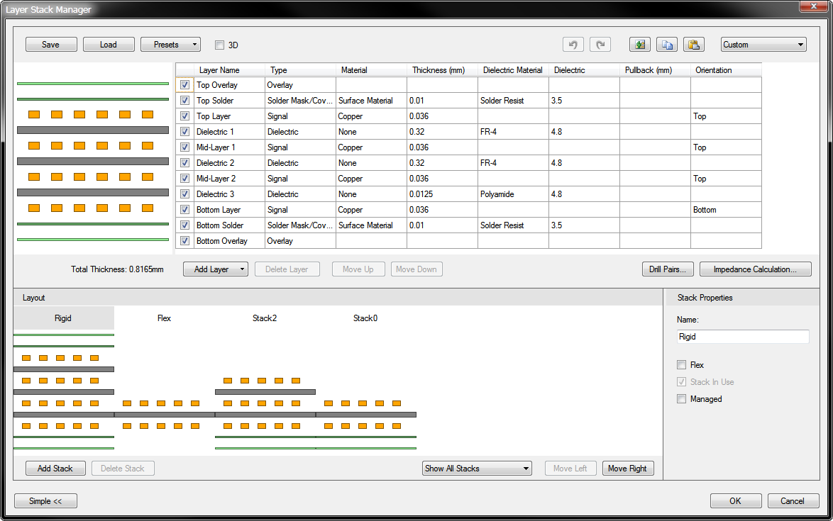
The Layer Stack Manager set to Show All Stacks revealing two Managed Stacks, Stack0 and Stack1.
Like User Stacks, Managed Stacks are listed in the PCB panel when it is set to Layer Stack Regions. The image below shows the managed stacks for two embedded components, R1 and C15.
Examining the Layer Stacks, the two Managed Stacks are visible on the right.