PCB Layer Stack Management
Contents
- PCB Layer Stackup Technology and Terminology
- A Single Design with Multiple Layer Stacks
- Defining the Layer Stack in the Layer Stack Manager
- Adding, Removing and Configuring the Layer Stacks
- Adding and Removing Layers from a Stack
- Configuring the Layer Properties
- Layer Types, Properties and Function
- Assigning a Net to a Plane Layer
- Defining the Overall Board Shape
- Defining a Board Region and Assigning a Sub-Stack
- Managed Stacks and Embedded Components
- Documenting the Layer Stack
- Configuring the Drill Pairs
- Including a Drill Table
A printed circuit board, or PCB, is used to mechanically support and electrically connect electronic components. An Austrian scientist, Dr Paul Eisler, is credited with making the first operational printed wiring board in 1943, where the printed circuits replaced the bulky wiring in a vacuum tube radio.
The PCB is designed and formed as a stack of layers. In the early days of printed circuit board (PCB) manufacturing, the board was simply an insulating core layer, clad with a thin layer of copper on one or both sides. Wiring was formed in the copper layer(s) as conductive traces, by etching away (removing) unwanted copper.

A simple, single-sided PCB. Note how the circuit tracks that are on the bottom layer are visible through the board.
Fast forward to today, where almost all PCB designs have multiple copper layers. Two to ten copper layers are common, but it is possible to fabricate a board with over thirty copper layers. These copper layers are defined in the design environment as part of the layer stack, along with the insulation material that separates them.
To design a single printed circuit board it is only necessary to define a single layer stack, which defines the entire board area in the vertical direction, or Z plane. However, technological innovation and refinements in the processing technology has led to a number of revolutionary concepts in PCB fabrication, including the ability to design and manufacture flexible PCBs. By joining rigid sections of PCB together via flexible sections, complex, hybrid PCBs can be designed, that can be folded to fit into unusually shaped enclosures.
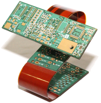
Rigid sections of PCB connected via flexible sections of PCB, an innovative concept that supports the design of creative and compact electronic products.
Since it is fabricated as a single entity, a rigid-flex PCB must be designed as a single entity. To do this, the designer must be able to define multiple PCB layer stacks, and assign different layer stacks to different parts of the rigid-flex design.
PCB Layer Stackup Technology and Terminology
Main article: PCB Layer Stackup Technology and Terminology
PCB technology has been driven not only by the quest for smaller electronic products, a leading driver of PCB technology has also been the quest for more compact components to use in those products. PGA and BGA components, with their array of interconnects are often fabricated using an internal PCB. It's the technology developed for this PCB, often referred to as High Density Interconnect (HDI) technology, that is now making its way into mainstream PCB fabrication.

An example of the internal structure of a Ball Grid Array package.
A Single Design with Multiple Layer Stacks
Like a simple, rigid PCB, a rigid-flex PCB is fabricated as a single entity. To be able to do this, the designer must be able to:
- Define the overall shape of the rigid-flex PCB.
- Define a master set of layers that includes all layers needed in the rigid-flex design.
- Define multiple layer stacks, where each stack includes only the layers needed for each of the rigid and flexible zones of the PCB.
- Define the different rigid and flexible zones where each sub-stack is applied.
- Generate detailed output fabrication and documentation files needed to fabricate the rigid-flex PCB.
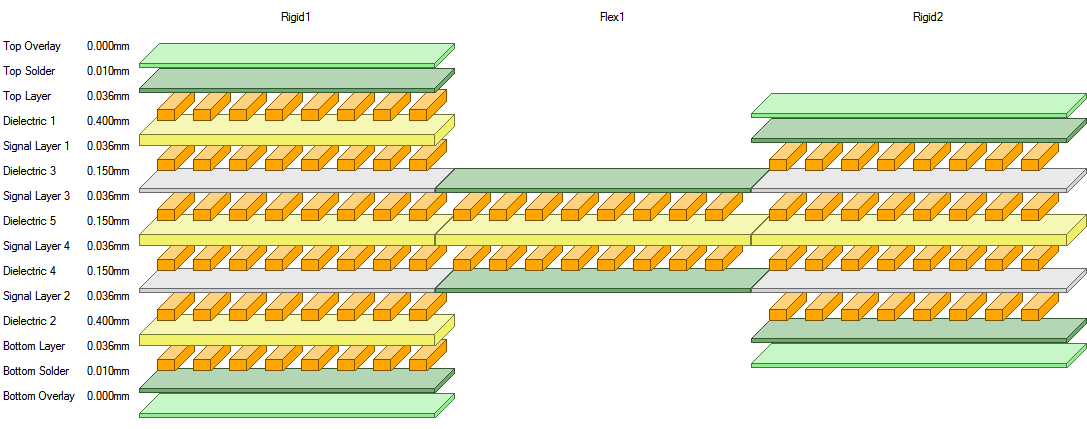
This board has had 3 layer stacks defined, 2 Rigid stacks and 1 Flex stack.
Defining the Layer Stack in the Layer Stack Manager
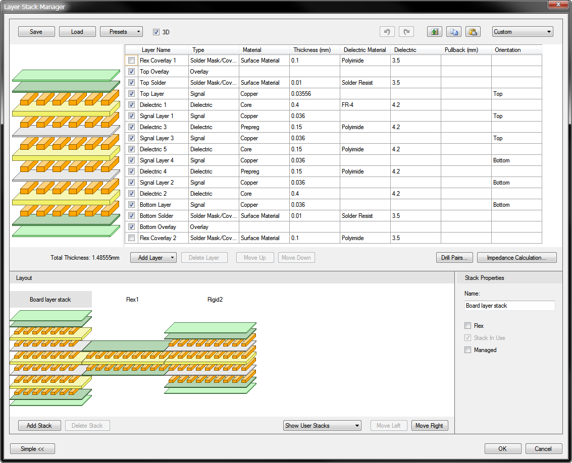
All layer stacks are defined in the Layer Stack Manager. To open the Layer Stack Manager select Design » Layer Stack Manager from the menus. For a new board, its single default stack comprises: a dielectric core, 2 copper layers, as well as the top and bottom solder/coverlay and overlay layers, as shown in the image below.
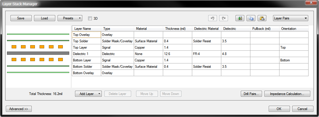
Layer stack management is performed in the Layer Stack Manager dialog. The default single stack for a new board is shown.
The dialog has two modes. In its Simple mode, the dialog provides the features and functionality needed to manage the layers in the stack for a traditional rigid PCB. For rigid-flex PCBs, you need to be able to create and manage multiple stacks. This is performed by entering the dialog's Advanced mode - by clicking the Advanced button at the bottom-left of the dialog.
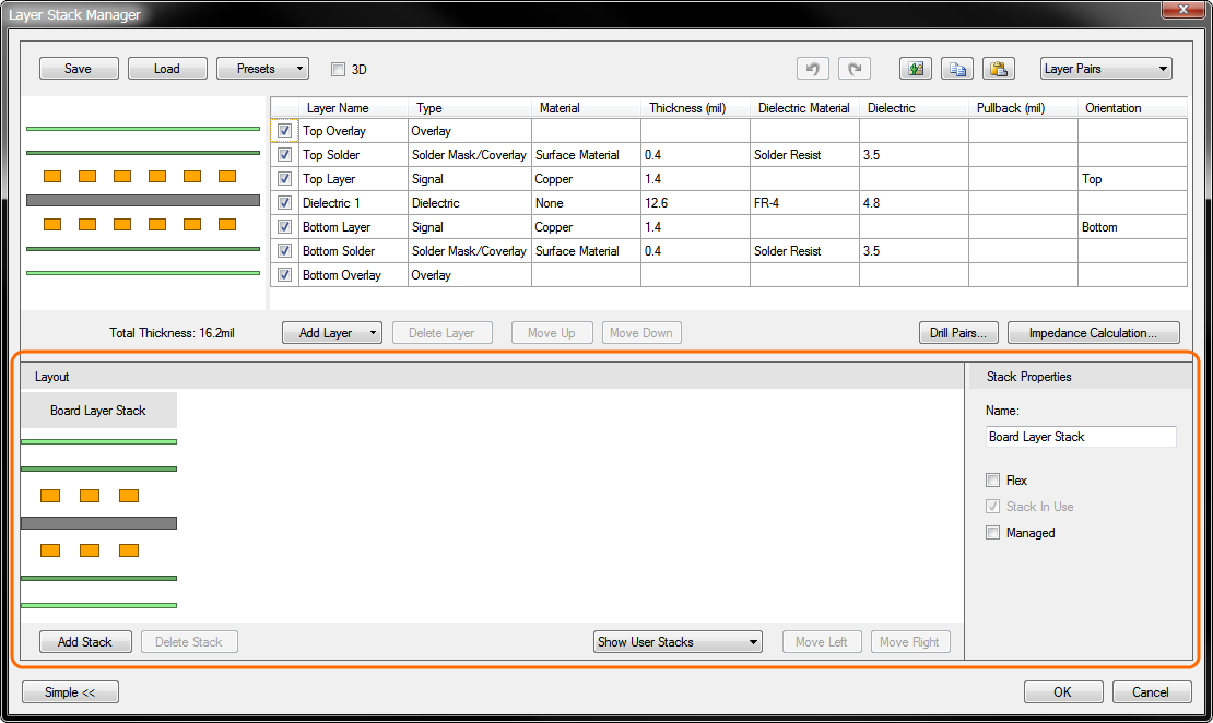
Controls for adding and managing stacks are made available by entering the dialog's Advanced mode, which displays the lower Stack region of the dialog.
In this mode, the dialog is visually and functionally divided into two key regions:
- Stack region (the lower region) – providing controls to add, delete and re-order layer stacks.
- Layer region (the upper region) – providing controls to manage the layers available to the defined stacks (add, remove, enable/disable, and re-order layers, as well as defining layer properties).
Adding, Removing and Configuring the Layer Stacks
Stacks are added, removed and their order is configured in the lower half of the Layer Stack Manager. Note that this section is only displayed if the ![]() button has been clicked.
button has been clicked.
Notes about adding, removing and configuring stacks:
- A single, default Board layer stack is defined when a new board is created. Note that this stack cannot be deleted, but it can be renamed.
- When the Add Stack button is clicked, the currently selected stack is duplicated and added to the right of the selected stack.
- Layer properties apply to the entire layer, across all stacks that the layer is a member of. Note that separate Solder Mask/Coverlay and Overlay layers can be added for each stack, if required.
- The order of the stacks, from left to right, can be changed using the Move Left and Move Right buttons at the bottom-right of the stack region. Note that the order that the stacks are shown in the Layer Stack Manager does not dictate how they are used in the board design.
- Each stack should be named to uniquely identify it, this helps ensure the correct stack is applied to each user-defined board region.
- Each stack that is flexible must have its Flex option enabled, so that required flex bending properties can be applied. Note that flex bending is defined by placing a Bending Line across the flex region (Design » Board Shape menu), and then editing its properties in the PCB panel when the panel is set to Layer Stack Regions mode.
A board with a total of 3 stacks defined, 2 rigid stacks and 1 flex stack.
Adding and Removing Layers from a Stack
Layers are added, removed and re-ordered in the upper half of the Layer Stack Manager using either the Add Layer button (for adding) or the right-click menu (for all types of changes).
Notes about adding, removing and moving layers:
- To add a new layer, click the Add Layer button and choose the type of layer to add (signal layer, internal plane, dielectric, or overlay).
- New layers are added into the set of layers listed in the upper part of the Layer Stack Manager. By default a newly added layer is enabled for use across all existing stacks. Simply select each stack in turn and disable the layer if it is not required in that stack, using the checkbox to the left of a layer's name.
- Note that this behavior, to automatically add a layer to all stacks, does not occur if Solder Mask/Coverlay and Overlay layers are added. These layer types can be added/removed to each stack.
- Initially, when a copper layer (signal or plane) is added, a dielectric layer is automatically added too, maintaining the symmetry of the stack (copper-dielectric-copper-dielectric, and so on). The location and type of dielectric that is added is controlled by the technology style setting, located at the top-right of the dialog. This is not the case if the style option is set to Custom, in this case only the chosen layer type is added (more details on the style setting below).
- To move a layer up or down in the stack, right-click on the layer and select the Move Layer Up or Move Layer Down command, or use Move Up or Move Down buttons. Note that when a copper or dielectric layer is moved the adjacent dielectric/copper layer will also move unless the style option is set to Custom, then only the selected layer will move.
- Layer Properties apply to the entire layer, across all stacks that the layer is a member of. This does not apply to Solder Mask/Coverlay and Overlay layers that have been selectively added to a stack.
- One or more layers can be selected and deleted. A deleted layer is removed from the set of available layers, and therefore removed from all stacks currently using it.
- Use the Undo and Redo buttons to roll layer stack changes backward or forward.
Configuring the Layer Properties
The properties of each layer must be completely defined, which should be done in consultation with the PCB fabricator. This information is included in the Layer Stack Table, the properties of each layer are edited directly in the layers region of the dialog. To edit a cell double-click on it, if that cell supports editing it will become available for editing.
Multi-cell editing is supported, to do this:
- Use the Windows standard Shift+Click (for a range) or Ctrl+Click (for individual cells) to select multiple cells.
- Press F2 to enter editing mode (do not use the mouse, or you will loose your selection).
- Use the keyboard to type the required string, or use the mouse to select the required option from a dropdown.
- For checkboxes, Shift+Click or Ctrl+Click in the cell around the checkbox, then press the Spacebar to toggle the setting of the selected checkboxes.
Layer Types, Properties and Function
In Altium Designer there is a single set of layers defined, and any layer can then be used in any layer stack. This set of layers includes all of the layers that are used in the overall PCB design, regardless of whether the design is a single PCB, or a rigid-flex design incorporating numerous rigid and flex sections. A variety of types of layers can be included in the layer stack: including copper, dielectric, surface finish and mask layers. Each layer must be completely specified in terms of its material and mechanical requirements, including: the material used, the thickness, the dielectric constant, and so on. The selection of materials and their properties should always be done in consultation with the board fabricator.
The layer types and their properties are detailed in the table below, the process of defining the required layers and assigning them to the various stacks, follows that.
| Layer Type | Material | Thickness | Properties to Define | Comments |
|---|---|---|---|---|
| Signal | Copper | mm or mils | Thickness | Copper layer used to define signal routing, carries the electrical signals and circuit supply current. Typically annealed foil and electro-deposited. |
| Internal Plane | Copper | mm or mils | Thickness | Solid copper layer used to distribute power and ground, can be split into regions. Also must specify the distance from the plane edge to the board edge (pullback). Typically annealed foil. |
| Dielectric | Varies, including: FR4, polyimide, and a variety of manufacturer-specific materials offering different design parameters | mm or mils | Type (function), Material, Thickness and Dielectric Constant (Dk). | Insulating layer, can be rigid or flexible. Used to define core, prepreg and flexible layers. Important mechanical properties include; including dimensional stability over moisture and temp ranges, tear resistance, flexibility. Important electrical properties include; insulation resistance, dielectric constant (Dk), dissipation factor (loss tangent, Df or Dj) |
| Overlay | Screen printed epoxy, LPI (liquid photoimageable) | Present text/artwork, such as component designators. | ||
| Solder Mask/Coverlay | 1) Liquid photoimageable solder mask (LPI or LPSM) , Dry Film photoimageable Solder Mask (DFSM), or 2) Adhesive coated flexible film, typically polyimide or polyester. | mm or mils | Type (function), Material, Thickness and Dielectric Constant (Dk). | 1) Protective layer that restricts where solder can be applied to the circuit. A cost effective and proven technology, suitable for rigid and flex use class A (flex-to-install) applications. Suitable for finer features than flexible film coverlay. 2) Suitable for flex use classes A and B (dynamic flex). Requires rounded holes/corners, which are typically drilled or punched. |
| Paste Mask | Layer from which a paste mask stencil is fabricated. Stencil is typically stainless steel. Openings in the stencil define locations where solder paste is to be applied to the component pads, prior to component placement. | Mask layer used to fabricate solder mask screen, which defines locations where solder paste is to be applied. |
Assigning a Net to a Plane Layer
Main Article: Internal Power and Split Planes
In earlier versions of Altium Designer, a net could be assigned to a plane either through the Layer Stack Manager, or by double-clicking on the plane layer in the workspace. With the introduction of multiple layer stacks, the net is always assigned to the plane by double-clicking on the plane layer in the workspace (the plane layer must be the active layer). When you double-click the Split Plane dialog will open, select the required net, as shown in the image below. This process is the same if you are assigning a single net to the entire plane, or are assigning a net to a split region of the plane.
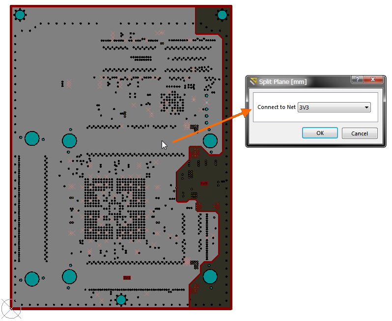
To assign a net to a plane layer, make the plane layer the active layer then double-click to open the Split Plane dialog, where the net is assigned.
Defining the Overall Board Shape
Main Article: Creating and Modifying the Board Shape
Regardless of the final make up of the board (single rigid area or multiple rigid-flex sections), the overall outer shape is defined as the Board Shape. The Board Shape can be:
- Defined manually - by redefining the shape, or moving the existing board vertices (corners). Switch to Board Planning Mode (View » Board Planning Mode) then use the commands in the Design menu.
- Defined from selected objects - typically done from an outline on a mechanical layer. Use this option if an outline has been imported from another design tool. Switch to 2D Layout Mode (View » 2D Layout Mode) then use the command in the Design » Board Shape sub-menu.
- Defined from a 3D body - use this option if the blank board has been imported as a STEP model from an MCAD tool into an Altium Designer 3D Body Object (Place » 3D Body). Switch to 3D Layout Mode (View » 3D Layout Mode) then use the command in the Design » Board Shape sub-menu to select the board shape.
Defining a Board Region and Assigning a Sub-Stack
Main Article: Defining Board Regions and Bending Lines
When a new board is created, the overall board shape is automatically assigned the board region called Default Layer Stack Region. Double-click anywhere within the board shape to open the Board Region dialog and change the default name. This default board region is automatically assigned the default Board layer stack. Note that the default Board layer stack is named in the Layer Stack Manager.
The board can be divided into regions by switching to the Board Planning Mode (View » Board Planning Mode, shortcut: 1) and defining Split Lines (Design menu). To learn more, refer to the article Defining Board Regions and Bending Lines.
Managed Stacks and Embedded Components
Related article: Designing with Embedded Components
When you embedded a component, Altium Designer has to manage how that embedded component affects the layer stack, not only in terms of how it is displayed, but also in terms of calculated data such as solder mask openings and design rule checking. It does this by creating a stack for each unique combination of placed + cut layers needed by the various embedded components included in the design. These stacks are referred to as Managed Stacks.
The Managed Stack is created automatically when a component is embedded within the layers of the board. As managed stacks are created automatically there is no user-input needed in their creation and management. Altium Designer checks for embedded components, tests if any of the current managed stacks are suitable and if not, creates a new one. The same applies when embedded components are removed, if a managed stack is no longer needed, it is automatically removed. To force Altium Designer to check if new managed stacks are needed, switch between 2D and 3D Layout Modes.
The image below shows the layer stack dialog for a rigid-flex design that includes embedded components. By analyzing the Managed Stacks it is possible to work out which layers the components are embedded on.
Note that:
- The stack selector down the bottom of the dialog is set to Show All Stacks, displaying the two managed stacks, Stack0 and Stack2. Note that the stack selector setting is not persistent, when the dialog is reopened it defaults to Show User Stacks.
- The upper-most layer in Stack2 is Mid-Layer 1, there are no other layers above this layer. This indicates that the upper layers are removed by the cutout (cavity definition) in the component embedded on Mid-Layer 1.
- The upper-most layer in Stack0 is Mid-Layer 2, there are no other layers above this layer. This indicates that the upper layers are removed by the cutout (cavity definition) in the component embedded on Mid-Layer 2.
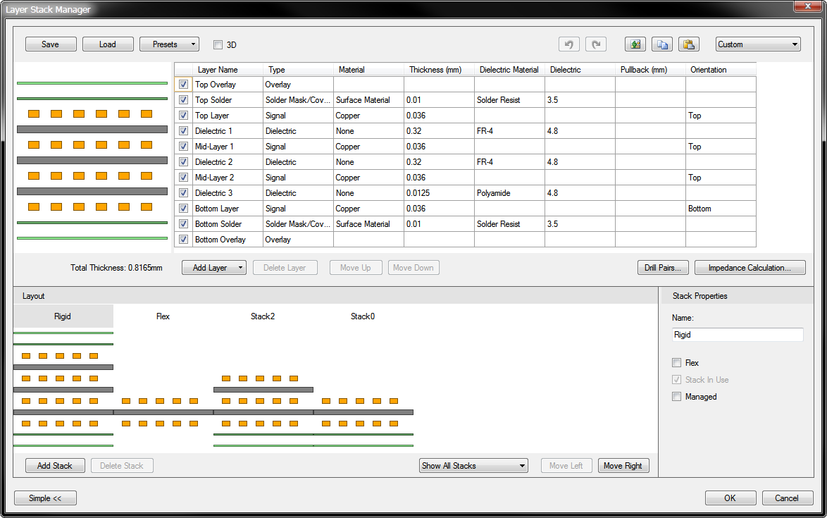
The Layer Stack Manager set to Show All Stacks revealing two Managed Stacks, Stack0 and Stack1.
Documenting the Layer Stack
Main Article: Documenting the Layer Stack
Documentation is a key part of the design process, and is particularly important for designs with a complex layer stack structure, such as a rigid-flex design. To support this, Altium Designer includes a Layer Stack Table, which is placed (Place » Layer Stack Table) and positioned alongside the board design in the workspace. The Layer Stack Table details the:
- Layers used in the design
- Material used for each layer
- Thickness of each layer
- The Dielectric Constant
- The name of each stack and the layers used in that stack
The Layer Stack Table can also include an optional map of the PCB, this is an outline of the board showing how the various layer stacks are assigned to regions of the board. The map can be scaled, or hidden if required.
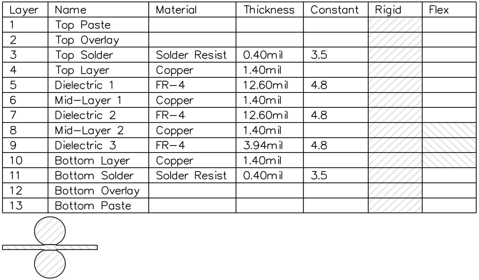
The Layer Stack Table is used to provide detail documentation of all layers used in the design, note the map included below the table.
Configuring the Drill Pairs
In a design with multiple layer stacks, the Drill Pairs are defined for each stack. Drill pairs are configured in the Layer Stack Manager.
To define the drill pairs:
- Select the stack in the lower part of the Layer Stack Manager.
- Click the Drill Pairs button to open the Drill-Pair Manager.
- Define the drill pairs for that stack, as required.
- Repeat the process for each Stack in the design.
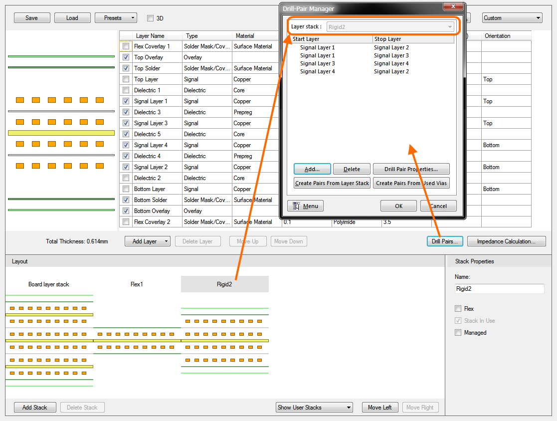
Select the stack then click the Drill Pairs button to define the drill pairs for that stack.
Including a Drill Table
Main Article: Live Drill Drawing Table
Altium Designer includes an intelligent Drill Table, which is placed like any other design object. The table displays the drills required for a specified layer pair, you will need to place a drill table for each layer pair used in the design.
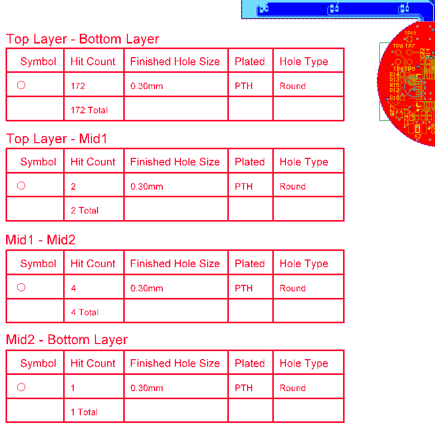
4 Drill Tables have been placed, one for each of the drill pairs defined in this rigid-flex design. A title has been added to each to identify the layer pair.