A via shield is used to create a vertical copper barrier through the PCB, to help reduce crosstalk and electromagnetic interference in a route that is carrying an RF signal. A via shield, also known as a via fence or a picket fence, is created by placing one or more rows of vias alongside a signal route. In the image below the net has been shielded by 2 rows of vias.
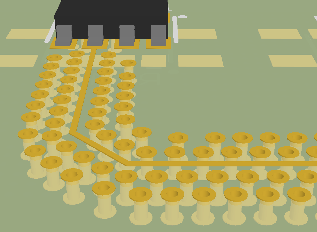
A net shielded with 2 rows of vias.
Placing a Via Shield
To place a via shield in Altium Designer, select Tools » Via Stitching/Shielding » Add Shielding to Net from the menus. The Add Shielding to Net dialog will appear, as shown below:
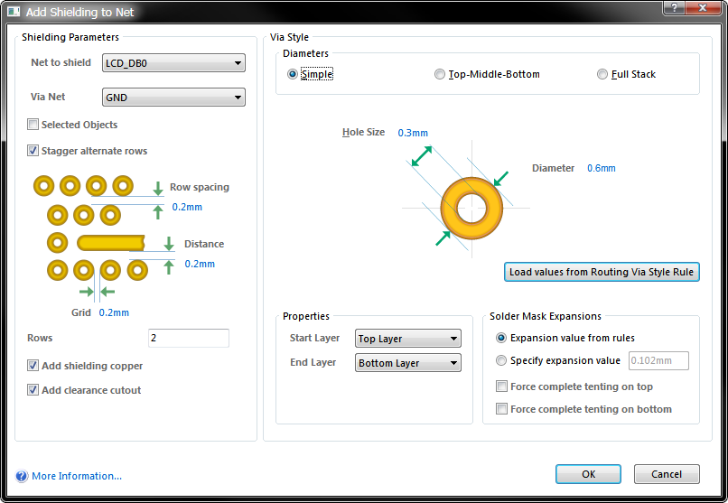
Configure the shielding via requirements, including their spacing, clearance and the number of rows.
Selecting Suitable Via Parameters
The size and positioning of the vias is not an exact science, but there are guidelines that have been established based on empirical testing.
As noted in the discussion forum(5) referenced below, for a PCB with an on-board antenna, "the distance between vias should be 1/4 your resonant wavelength at the most."
The forum discussion also references a technical note(6), which states that "the common rule of thumb is to locate stitch vias no further apart than λ/10 and preferably as often as λ/20."
Including Shielding Copper with the Stitching
As well as adding shielding vias along each side of the routing, you can also include shielding copper, as shown in the image below. To do this, enable the Add shielding copper option. This copper is created as a polygon, so it obeys the applicable Clearance and Polygon Connect Style design rules. To give better control of keeping this shielding copper away from the shielded net, the Add Shielding to Net dialog includes an Add clearance cutout option. When this option is enabled a polygon cutout is placed around the shielded net, with its edge set back from the routing at the same Distance as the shielding vias.

Shielding vias around a net, with shielding copper and a clearance cutout.
Further Reading
- For information about all aspects of PCB design, refer to the Printed Circuit Design and Fab Magazine website. The site is an excellent resource for technical topics, such as the role of a "via fence" (include the quote marks to improve the quality of the search results).
- Wikipedia article, Via Fence
- Studies on Via Coupling on Multilayer Printed Circuit Boards
- A paper that introduces the basic principals of EM wave propagation within a PCB structure - Best practice in circuit board design
- A discussion forum where the question Via fences for noise reduction of a chip antenna? was asked
- An interesting technical note that gives rule of thumb guidelines on stitch via spacing
- PCB design techniques for lowest-cost EMC compliance: part 1’ M K Armstrong. Electronics & Communications Engineering Journal Vol 11 No 4. IEE, August 1999.