Altium Designer 14.3 incorporates a number of additions and enhancements to both the IPC®-Compliant Footprint Wizard, and the IPC®-Compliant Footprints Batch Generator. These changes are aimed at making both truly compliant with Revision B of the IPC standard 7351 - Generic Requirements for Surface Mount Design and Land Pattern Standard.
The following additional packages are now supported: CAPAE, CHIP ARRAY, DFN, LGA, PQFN, PSON, SODFL, SON, and SOTFL. In addition, existing packages have been reviewed and modified with respect to data required and/or terminology, with graphics enhanced to better illustrate the application of that data.
Three further beneficial enhancements have also been added in this release:
- Splitting of the paste mask into small fills, for packages with a large thermal pad (sized 2.1mm x 1.6mm, or larger).
- For packages involving gullwing leads, pads are trimmed to prevent them from otherwise extending under the package's body.
- For small packages having a large central thermal pad (PQFP, QFN, SOIC, SOP), the peripheral pads are trimmed to ensure required clearance between the pads, in accordance with the IPC Standard.
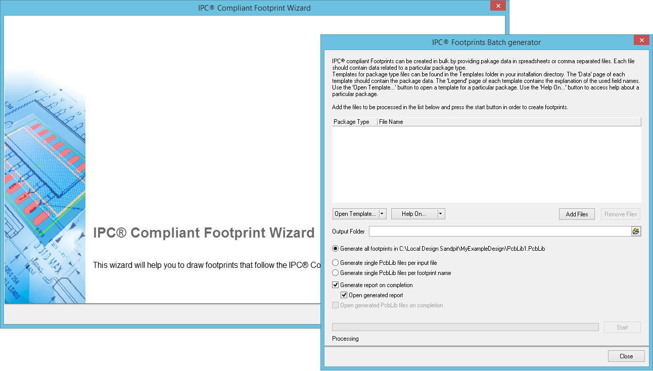
Create PCB library components compliant with IPC standard 7351B - individually, or en-masse - using the enhanced IPC®-Compliant Footprint Wizard and IPC®-Compliant Footprints Batch Generator.
Newly Supported Packages
The following sections detail the new packages introduced in Altium Designer 14.3, and supported in both the IPC-Compliant Footprint Wizard and the IPC-Compliant Footprints Batch Generator.
CAPAE
Description: Electrolytic Aluminum Capacitor
Included Packages: CAPAE
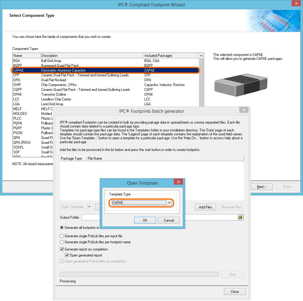
Support for CAPAE packages, added to the IPC-Compliant Footprint Wizard and IPC-Compliant Footprints Batch Generator.
The following tables list the information (required and optional) when defining the CAPAE package in an Excel file for use with the IPC-Compliant Footprints Batch Generator. Similar required information will be reflected in the corresponding pages of the IPC-Compliant Footprint Wizard.
Table of data related to CAPAE Package Specifications.
| Name | Value Required | Format | Description (Dimensions in mm) |
|---|---|---|---|
| FootprintName | Optional | String | If blank, then auto-generated IPC naming will be used |
| FootprintDescription | Optional | String | If blank, then description is auto-generated |
| Lmin, Lmax | Yes | Real | Minimum and maximum lead span |
| Wmin, Wmax | Yes | Real | Minimum and maximum body width |
| Tmin, Tmax | Yes | Real | Minimum and maximum length of lead |
| Twmin, Twmax | Yes | Real | Minimum and maximum width of lead |
| Amin | Optional | Real | Minimum component height |
| Amax | Yes | Real | Maximum component height |
| L1min, L1max | Yes | Real | Minimum and maximum body length |
| Dmax,Dmin | Yes | Real | Diameter of Body |
| DensityLevel | Optional | L, M, N | M = Most or maximum copper (density level A), N = Nominal or median copper (density level B), L = Least or minimum copper (density level C) |
| JHmin | Optional | Real | Minimum value for heel fillet |
| JSmin | Optional | Real | Minimum value for side fillet |
| JTmin | Optional | Real | Minimum value for toe fillet |
| DrawingNote | Optional | String | If package has other features that will affect the footprint, then enter details. |
Table of data related to CAPAE Footprint Specifications.
| Name | Value Required | Format | Description (Dimensions in mm) |
|---|---|---|---|
| Z | Optional | Real | Distance between pads. Measured from outside edges |
| G | Optional | Real | Distance between pads. Measured from inside edges |
| X | Optional | Real | Pad width |
| Y | Optional | Real | Pad length |
| C | Optional | Real | Row spacing. Distance between pad centers |
| A | Optional | Real | Assembly width |
| B | Optional | Real | Assembly length |
| V1 | Optional | Real | Courtyard width |
| V2 | Optional | Real | Courtyard length |
| R1 | Optional | Real | Silkscreen width |
| R2 | Optional | Real | Silkscreen length |
Chip Array
Description: Chip Array
Included Packages: Chip Array, Chip Array Exposed Pad
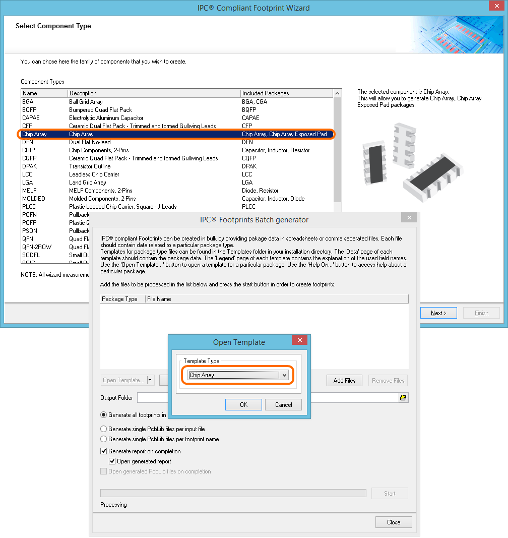
Support for Chip Array packages, added to the IPC-Compliant Footprint Wizard and IPC-Compliant Footprints Batch Generator.
The following tables list the information (required and optional) when defining the Chip Array package in an Excel file for use with the IPC-Compliant Footprints Batch Generator. Similar required information will be reflected in the corresponding pages of the IPC-Compliant Footprint Wizard.
Table of data related to Chip Array Package Specifications.
| Name | Value Required | Format | Description (Dimensions in mm) |
|---|---|---|---|
| FootprintName | Optional | String | If blank, then auto-generated IPC naming will be used |
| FootprintDescription | Optional | String | If blank, then description is auto-generated |
| Emin, Emax | Yes | Real | Minimum and maximum body width |
| Dmin, Dmax | Yes | Real | Minimum and maximum body length (side containing pin 1) |
| Bmin, Bmax | Yes | Real | Minimum and maximum lead width |
| B1min, B1max | Optional | Real | Minimum and maximum corner lead width |
| Lmin, Lmax | Yes | Real | Minimum and maximum lead length |
| Amax | Yes | Real | Maximum height |
| Amin | Optional | Real | Minimum height |
| PinCount | Yes | Integer | Total number of pin positions (including absent pins) |
| Pitch | Yes | Real | Pitch (e) |
| PackageType | Yes | Flat,Concave,ConvexE, ConvexS | Type of packge |
| DensityLevel | Optional | L, M, N | M = Most or maximum copper (density level A), N = Nominal or median copper (density level B), L = Least or minimum copper (density level C) |
| JHmin | Optional | Real | Minimum value for heel fillet. |
| JSmin | Optional | Real | Minimum value for side fillet. |
| JTmin | Optional | Real | Minimum value for toe fillet. |
| DrawingNote | Optional | String | If package has other features that will affect the footprint, then enter details. |
Table of data related to Chip Array Footprint Specifications.
| Name | Value Required | Format | Description (Dimensions in mm) |
|---|---|---|---|
| Z | Yes | Real | Distance between pads. Measured from outside edges |
| C | Optional | Real | Row spacing. Distance between pad centers |
| G | Yes | Real | Distance between pads. Measured from inside edges |
| X | Yes | Real | Pad width |
| X1 | Optional | Real | Corner pad width |
| Y | Yes | Real | Pad length |
| A | Yes | Real | Assembly width (E side) |
| B | Yes | Real | Assembly length (D side) |
| V1 | Yes | Real | Courtyard width (E side) |
| V2 | Yes | Real | Courtyard length (D side) |
| R1 | Yes | Real | Silkscreen width (E side) |
| R2 | Yes | Real | Silkscreen length (D side) |
DFN
Description: Dual Flat No-lead
Included Packages: DFN
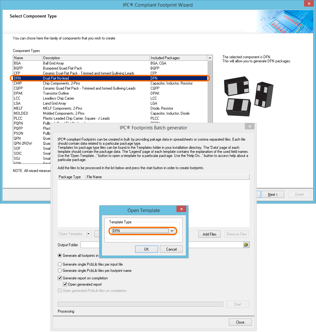
Support for DFN packages, added to the IPC-Compliant Footprint Wizard and IPC-Compliant Footprints Batch Generator.
The following tables list the information (required and optional) when defining the DFN package in an Excel file for use with the IPC-Compliant Footprints Batch Generator. Similar required information will be reflected in the corresponding pages of the IPC-Compliant Footprint Wizard.
Table of data related to DFN Package Specifications.
| Name | Value Required | Format | Description (Dimensions in mm) |
|---|---|---|---|
| FootprintName | Optional | String | If blank, then auto-generated IPC naming will be used |
| FootprintDescription | Optional | String | If blank, then description is auto-generated |
| Emin, Emax | Yes | Real | Minimum and maximum body width |
| Dmin, Dmax | Yes | Real | Minimum and maximum body length (side containing pin 1) |
| b1min, b1max | Yes | Real | Minimum and maximum lead width (small lead) |
| L1min, L1 max | Yes | Real | Minimum and maximum lead length (small lead) |
| Amax | Yes | Real | Maximum height |
| Amin | Optional | Real | Minimum height |
| A1max | Optional | Real | Maximum standoff height |
| A1min | Yes | Real | Minimum standoff height |
| PinCount | Yes | Integer | Total number of pin positions (2,3,4) |
| e1 | Optional | Real | Pitch (e1) |
| e2 | Yes | Real | Pitch (e2) |
| e | Optional | Real | Pitch (e) |
| b2min, b2max | Yes | Real | Minimum and maximum lead width (big lead) |
| L2min, L2max | Yes | Real | Minimum and maximum lead length (big lead) |
| DensityLevel | Optional | L, M, N | M = Most or maximum copper (density level A), N = Nominal or median copper (density level B), L = Least or minimum copper (density level C) |
| DrawingNote | Optional | String | If package has other features that will affect the footprint, then enter details. |
Table of data related to DFN Footprint Specifications.
| Name | Value Required | Format | Description (Dimensions in mm) |
|---|---|---|---|
| A | Yes | Real | Assemble width (D side) |
| B | Yes | Real | Assemble length (E side) |
| C | Yes | Real | pads span betwen small one |
| C1 | Yes | Real | pads span between big and samll one |
| C2 | Yes | Real | distance from package center to center of big pad |
| R1 | Yes | Real | Silkscreen width (D side) |
| R2 | Yes | Real | Silkscreen length (E side) |
| V1 | Yes | Real | Courtyard width (D side) |
| V2 | Yes | Real | Courtyard length (E side) |
| X1 | Yes | Real | Small pad width |
| Y1 | Yes | Real | Small pad length |
| X2 | Yes | Real | Big pad width |
| Y2 | Yes | Real | Big pad length |
LGA
Description: Land Grid Array
Included Packages: LGA
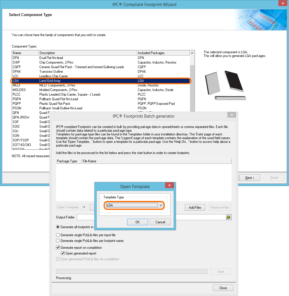
Support for LGA packages, added to the IPC-Compliant Footprint Wizard and IPC-Compliant Footprints Batch Generator.
The following tables list the information (required and optional) when defining the LGA package in an Excel file for use with the IPC-Compliant Footprints Batch Generator. Similar required information will be reflected in the corresponding pages of the IPC-Compliant Footprint Wizard.
Table of data related to LGA Package Specifications.
| Name | Value Required | Format | Description (Dimensions in mm) |
|---|---|---|---|
| FootprintName | Optional | String | If blank, then auto-generated IPC naming will be used |
| FootprintDescription | Optional | String | If blank, then description is auto-generated |
| Dmin, Dmax | Yes | Real | Minimum and maximum body length along D side (A, B, C, ...) |
| D1ave | Yes | Real | Average length of grid along D side |
| Emin, Emax | Yes | Real | Minimum and maximum body length along E side (1, 2, 3, ...) |
| E1ave | Yes | Real | Average length of grid along E side |
| A1min | Yes | Real | Minimum standoff height |
| A1max | Optional | Real | Maximum standoff height |
| A2min, A2max | Optional | Real | Minimum and maximum body height |
| Amin | Optional | Real | Minimum overall height |
| Amax | Yes | Real | Maximum overall height |
| Bnom | Yes | Real | Average lead size |
| LeadShape | Yes | R,S | Lead shape, round or square |
| PitchD, PitchE | Yes | Real | Distance between ball centres, in "D" and "E" directions |
| GridType | Yes | P, S | P = Plain Grid, S = Staggered Grid |
| MatrixType | Yes | F, P, SD, TE | F = Full Matrix, P = Perimeter, SD = Selectively Depopulated, TE = Thermally Enhanced |
| Rows | Yes | Integer | Number of balls along D side (A, B, C, ...) |
| Columns | Yes | Integer | Number of balls along E side (1, 2, 3, ...) |
| Nmax | Yes | Integer | Maximum number of ball positions (Rows x Columns) |
| PinCount | Yes | Integer | Number of actual balls present |
| DepopulateBalls | Optional | String | Ball positions removed from matrix. Example: C5-H10,B6-B9,A1 |
| RepopulateBalls | Optional | String | Ball positions added back into depopulated matrix. Example: C8,D6-F9 |
| DrawingNote | Optional | String | If package has other features that will affect the footprint, then enter details. |
Table of data related to LGA Footprint Specifications.
| Name | Value Required | Format | Description (Dimensions in mm) |
|---|---|---|---|
| X | Optional | Real | Diameter of pad. If specified this overrides the calculated value. This can be used to specify a manufacturer's recommended pad size. |
| C1 | Optional | Real | |
| C2 | Optional | Real | |
| A | Optional | Real | Assembly width |
| B | Optional | Real | Assembly length |
| V1 | Optional | Real | Courtyard width |
| V2 | Optional | Real | Courtyard length |
| R1 | Optional | Real | Silkscreen width |
| R2 | Optional | Real | Silkscreen length |
PQFN
Description: Pulback Quad Flat No-lead
Included Packages: PQFN
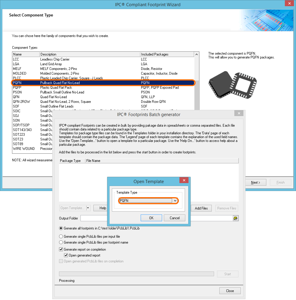
Support for PQFN packages, added to the IPC-Compliant Footprint Wizard and IPC-Compliant Footprints Batch Generator.
The following tables list the information (required and optional) when defining the PQFN package in an Excel file for use with the IPC-Compliant Footprints Batch Generator. Similar required information will be reflected in the corresponding pages of the IPC-Compliant Footprint Wizard.
Table of data related to PQFN Package Specifications.
| Name | Value Required | Format | Description (Dimensions in mm) |
|---|---|---|---|
| FootprintName | Optional | String | If blank, then auto-generated IPC naming will be used |
| FootprintDescription | Optional | String | If blank, then description is auto-generated |
| Dmin, Dmax | Yes | Real | Minimum and maximum body span on side D |
| Emin, Emax | Yes | Real | Minimum and maximum body span on side E |
| Bmin, Bmax | Yes | Real | Minimum and maximum lead width |
| Lmin, Lmax | Yes | Real | Minimum and maximum lead length |
| Amin | Optional | Real | Minimum height |
| Amax | Yes | Real | Maximum height |
| A1min | Yes | Real | Minimum standoff height |
| A1max | Optional | Real | Maximum standoff height |
| L1min, L1max | Yes | Real | Lead pull-back length |
| PinCountD | Yes | Integer | Number of pins on D side of package |
| PinCountE | Yes | Integer | Number of pins on E side of package |
| PitchD | Yes | Real | Distance between two adjacent pins on side D |
| PitchE | Yes | Real | Distance between two adjacent pins on side E |
| Pin1 | Yes | S2, C1 | Location of pin 1; S2 = corner of package. C1 = center of package side |
| D2min, D2max | Optional | Real | Minimum and maximum thermal pad size on D side. If there is no thermal pad leave this field blank |
| E2min, E2max | Optional | Real | Minimum and maximum thermal pad size on E side. If there is no thermal pad leave this field blank |
| DensityLevel | Optional | L, M, N | M = Most or maximum copper (density level A), N = Nominal or median copper (density level B), L = Least or minimum copper (density level C) |
| Periphery | Optional | Real | Land Periphery |
| DrawingNote | Optional | String | If package has other features that will affect the footprint, then enter details. |
Table of data related to PQFN Footprint Specifications.
| Name | Value Required | Format | Description (Dimensions in mm) |
|---|---|---|---|
| ZE | Optional | Real | Distance between pads. Measured from outside edges |
| ZD | Optional | Real | Distance between pads. Measured from outside edges |
| GE | Optional | Real | Distance between pads. Measured from inside edges |
| GD | Optional | Real | Distance between pads. Measured from inside edges |
| X | Optional | Real | Pad width |
| Y | Optional | Real | Pad length |
| CE | Optional | Real | Row spacing. Distance between pad centers |
| CD | Optional | Real | Row spacing. Distance between pad centers |
| E2t | Optional | Real | Thermal Pad width |
| D2t | Optional | Real | Thermal Pad length |
| L2 | Optional | Real | Power Bar width. |
| B2, B3, B4, B5, G3, G4, G5, G6 | Optional | Real | Power Bar length. If all are blank, no power bars are drawn. |
| A | Optional | Real | Assembly width (E side) |
| B | Optional | Real | Assembly length (D side) |
| V1 | Optional | Real | Courtyard width (E side) |
| V2 | Optional | Real | Courtyard length (D side) |
| R1 | Optional | Real | Silkscreen width (E side) |
| R2 | Optional | Real | Silkscreen length (D side) |
PSON
Description: Pulback Small Outline No-lead
Included Packages: PSON
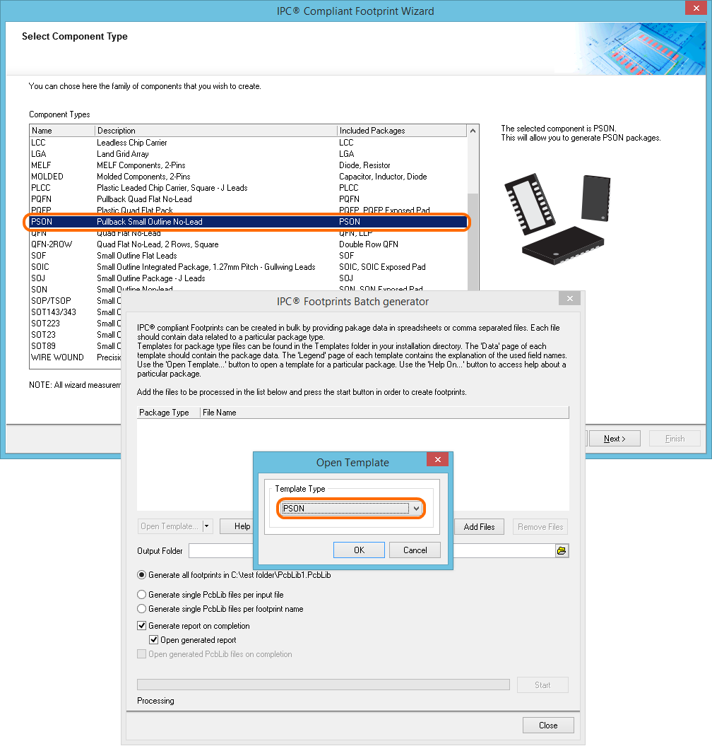
Support for PSON packages, added to the IPC-Compliant Footprint Wizard and IPC-Compliant Footprints Batch Generator.
The following tables list the information (required and optional) when defining the PSON package in an Excel file for use with the IPC-Compliant Footprints Batch Generator. Similar required information will be reflected in the corresponding pages of the IPC-Compliant Footprint Wizard.
Table of data related to PSON Package Specifications.
| Name | Value Required | Format | Description (Dimensions in mm) |
|---|---|---|---|
| FootprintName | Optional | String | If blank, then auto-generated IPC naming will be used |
| FootprintDescription | Optional | String | If blank, then description is auto-generated |
| Emin, Emax | Yes | Real | Minimum and maximum body width |
| Dmin, Dmax | Yes | Real | Minimum and maximum body length (side containing pin 1) |
| D2min, D2max | Optional | Real | Minimum and maximum thermal pad size on D side. If there is no thermal pad leave this field blank |
| E2min, E2max | Optional | Real | Minimum and maximum thermal pad size on E side. If there is no thermal pad leave this field blank |
| Bmin, Bmax | Yes | Real | Minimum and maximum lead width |
| cmin, cmax | Optional | Real | Minimum and maximum lead height |
| Lmin, Lmax | Yes | Real | Minimum and maximum lead length |
| L1min, L1max | Optional | Real | Minimum and maximum lead pullback |
| Amax | Yes | Real | Maximum height |
| Amin | Optional | Real | Minimum height |
| A1max | Optional | Real | Maximum standoff height |
| A1min | Yes | Real | Minimum standoff height |
| PinCount | Yes | Integer | Total number of pin positions (including absent pins) |
| Pitch | Yes | Real | Pitch (e) |
| AbsentPins | Optional | String | Comma separated list showing absent pins. Example: 1,2,5. If blank all pins present |
| PinOrder | Optional | String | Comma separated list showing pin order. If blank pin order is assumed sequential from 1 to PinCount. Example: 8,7,6,5,4,3,2,1 will reverse the pin order of an 8 pin package |
| DensityLevel | Optional | L, M, N | M = Most or maximum copper (density level A), N = Nominal or median copper (density level B), L = Least or minimum copper (density level C) |
| Periphery | Optional | Real | |
| DrawingNote | Optional | String | If package has other features that will affect the footprint, then enter details. |
Table of data related to PSON Footprint Specifications.
| Name | Value Required | Format | Description (Dimensions in mm) |
|---|---|---|---|
| Z | Yes | Real | Distance between pads. Measured from outside edges |
| C | Optional | Real | Row spacing. Distance between pad centers |
| G | Yes | Real | Distance between pads. Measured from inside edges |
| X | Yes | Real | Pad width |
| Y | Yes | Real | Pad length |
| E2t | Optional | Real | Thermal Pad width (X2) |
| D2t | Optional | Real | Thermal Pad length (Y2) |
| A | Yes | Real | Assembly width (E side) |
| B | Yes | Real | Assembly length (D side) |
| V1 | Yes | Real | Courtyard width (E side) |
| V2 | Yes | Real | Courtyard length (D side) |
| R1 | Yes | Real | Silkscreen width (E side) |
| R2 | Yes | Real | Silkscreen length (D side) |
| ViaCountE | Optional | Integer | Number of thermal vias in the E direction |
| ViaCountD | Optional | Integer | Number of thermal vias in the D direction |
| ViaPitchE | Optional | Real | Thermal Via Pitch in the E direction |
| ViaPitchD | Optional | Real | Thermal Via Pitch in the D direction |
| XY_Solder | Optional | Real | Peripheral Pads - Top Solder Layer. Enter expansion value for Solder Mask. Only enter value if following manufacturer recommendation. Otherwise leave blank |
| X2Y2_Solder | Optional | Real | Thermal Pad - Top Solder Layer. Enter expansion value for Solder Mask. Only enter value if following manufacturer recommendation. Otherwise leave blank |
| XY_Paste | Optional | Real | Peripheral Pads - Top Paste Layer. Enter expansion value for Paste Mask. Only enter value if following manufacturer recommendation. Otherwise leave blank. |
| X2Y2_Paste | Optional | Real | Thermal Pad - Top Paste Layer. Enter expansion value for Paste Mask. Only enter value if following manufacturer recommendation. Otherwise leave blank. |
| X_Paste | Optional | Real | Peripheral Pads - Fill on Top Paste Layer. Value in X direction. |
| Y_Paste | Optional | Real | Peripheral Pads - Fill on Top Paste Layer. Value in Y direction. |
| X2_Paste | Optional | Real | Thermal Pad- Fill on Top Paste Layer. Value in X direction. |
| Y2_Paste | Optional | Real | Thermal Pad- Fill on Top Paste Layer. Value in Y direction. |
| FillCountE | Optional | Integer | Number of Top Paste fills placed on the thermal pad in the E direction (No Paste Mask fills placed if blank) |
| FillCountD | Optional | Integer | Number of Top Paste fills placed on the thermal pad in the D direction (No Paste Mask fills placed if blank) |
| Fill_Gap | Optional | Real | Gap between Top Paste fills placed on the thermal pad (0.2mm if blank) |
SODFL
Description: Small Outline Diode, Flat Lead
Included Packages: SODFL
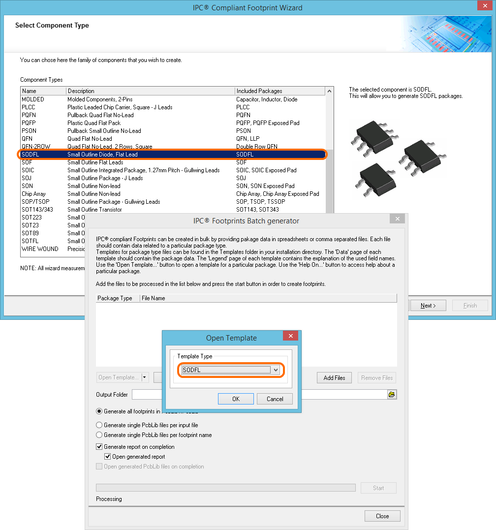
Support for SODFL packages, added to the IPC-Compliant Footprint Wizard and IPC-Compliant Footprints Batch Generator.
The following tables list the information (required and optional) when defining the SODFL package in an Excel file for use with the IPC-Compliant Footprints Batch Generator. Similar required information will be reflected in the corresponding pages of the IPC-Compliant Footprint Wizard.
Table of data related to SODFL Package Specifications.
| Name | Value Required | Format | Description (Dimensions in mm) |
|---|---|---|---|
| FootprintName | Optional | String | If blank, then auto-generated IPC naming will be used |
| FootprintDescription | Optional | String | If blank, then description is auto-generated |
| Dmin, Dmax | Yes | Real | Minimum and maximum body length |
| Emin, Emax | Yes | Real | Minimum and maximum lead span |
| E1min, E1max | Yes | Real | Minimum and maximum body width |
| Bmin, Bmax | Yes | Real | Minimum and maximum width |
| Lmin, Lmax | Yes | Real | Minimum and maximum lead length |
| Amin, Amax | Yes | Real | Minimum height |
| DensityLevel | Yes | L, M, N | M = Most or maximum copper (density level A), N = Nominal or median copper (density level B), L = Least or minimum copper (density level C) |
| JHmin | Optional | Real | Minimum value for heel fillet |
| JSmin | Optional | Real | Minimum value of side fillet |
| JTmin | Optional | Real | Minimum value for toe fillet |
| DrawingNote | Optional | String | If package has other features that will affect the footprint, then enter details. |
Table of data related to SODFL Footprint Specifications.
| Name | Value Required | Format | Description (Dimensions in mm) |
|---|---|---|---|
| Z | Optional | Real | Distance between pads. Measured from outside edges |
| C | Optional | Real | Distance between pads. Measured from pad centre |
| G | Optional | Real | Distance between pads. Measured from inside edges |
| X | Optional | Real | Pad width |
| Y | Optional | Real | Pad length |
| X1 | Optional | Real | Pad width (large pad) |
| A | Optional | Real | Assembly width |
| B | Optional | Real | Assembly length |
| V1 | Optional | Real | Courtyard width |
| V2 | Optional | Real | Courtyard length |
| R1 | Optional | Real | Silkscreen width |
| R2 | Optional | Real | Silkscreen length |
SON
Description: Small Outline No-lead
Included Packages: SON, SON Exposed Pad
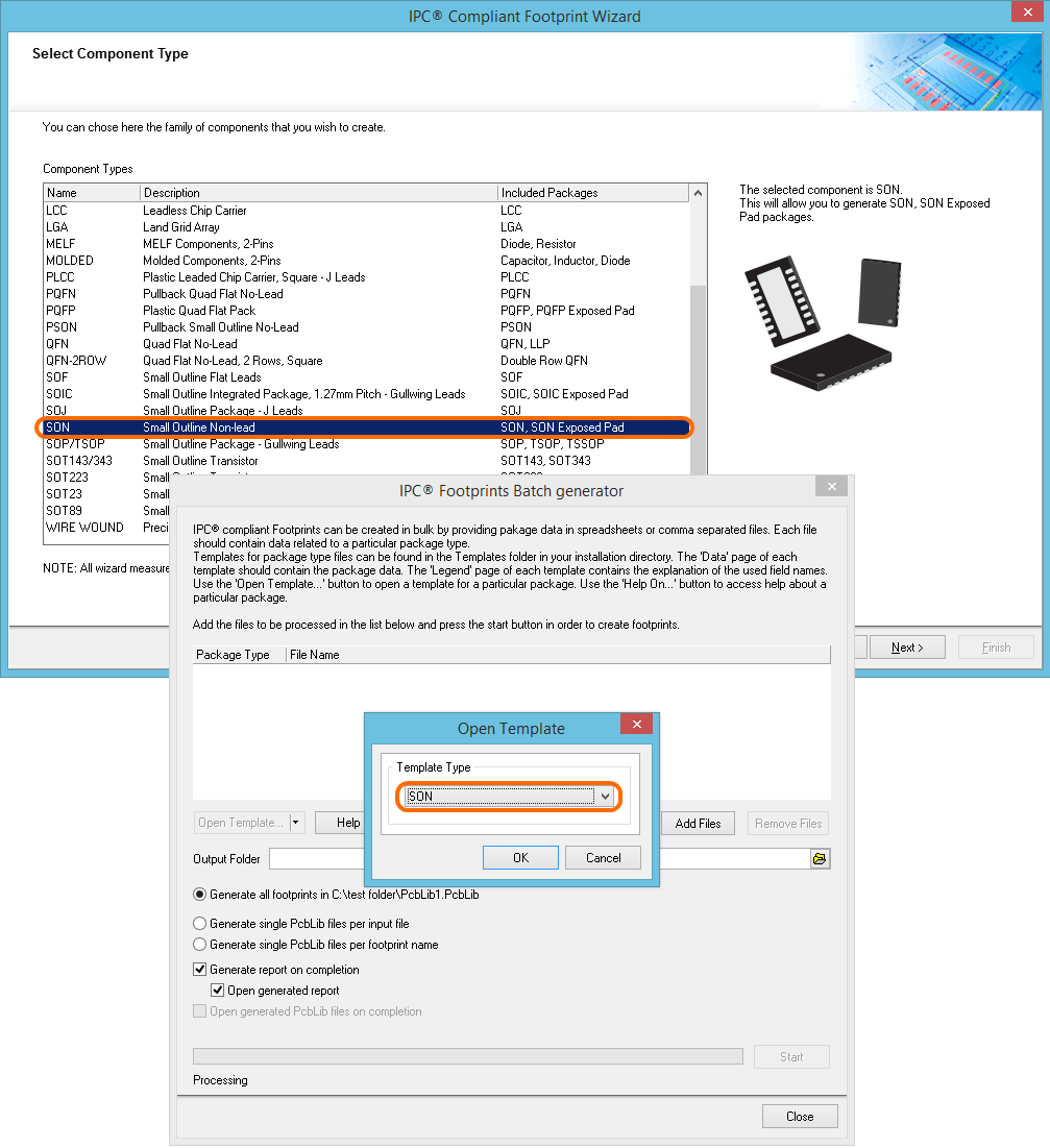
Support for SON packages, added to the IPC-Compliant Footprint Wizard and IPC-Compliant Footprints Batch Generator.
The following tables list the information (required and optional) when defining the SON package in an Excel file for use with the IPC-Compliant Footprints Batch Generator. Similar required information will be reflected in the corresponding pages of the IPC-Compliant Footprint Wizard.
Table of data related to SON Package Specifications.
| Name | Value Required | Format | Description (Dimensions in mm) |
|---|---|---|---|
| FootprintName | Optional | String | If blank, then auto-generated IPC naming will be used |
| FootprintDescription | Optional | String | If blank, then description is auto-generated |
| Emin, Emax | Yes | Real | Minimum and maximum body width |
| Dmin, Dmax | Yes | Real | Minimum and maximum body length (side containing pin 1) |
| D2min, D2max | Optional | Real | Minimum and maximum thermal pad size on D side. If there is no thermal pad leave this field blank |
| E2min, E2max | Optional | Real | Minimum and maximum thermal pad size on E side. If there is no thermal pad leave this field blank |
| Bmin, Bmax | Yes | Real | Minimum and maximum lead width |
| cmin, cmax | Optional | Real | Minimum and maximum lead height |
| Lmin, Lmax | Yes | Real | Minimum and maximum lead length |
| L1min, L1max | Optional | Real | Minimum and maximum lead pullback |
| Amax | Yes | Real | Maximum height |
| Amin | Optional | Real | Minimum height |
| A1max | Optional | Real | Maximum standoff height |
| A1min | Yes | Real | Minimum standoff height |
| PinCount | Yes | Integer | Total number of pin positions (including absent pins) |
| Pitch | Yes | Real | Pitch (e) |
| AbsentPins | Optional | String | Comma separated list showing absent pins. Example: 1,2,5. If blank all pins present |
| PinOrder | Optional | String | Comma separated list showing pin order. If blank pin order is assumed sequential from 1 to PinCount. Example: 8,7,6,5,4,3,2,1 will reverse the pin order of an 8 pin package |
| DensityLevel | Optional | L, M, N | M = Most or maximum copper (density level A), N = Nominal or median copper (density level B), L = Least or minimum copper (density level C) |
| JHmin | Optional | Real | Minimum value for heel fillet. |
| JSmin | Optional | Real | Minimum value for side fillet. |
| JTmin | Optional | Real | Minimum value for toe fillet. |
| DrawingNote | Optional | String | If package has other features that will affect the footprint, then enter details. |
Table of data related to SON Footprint Specifications.
| Name | Value Required | Format | Description (Dimensions in mm) |
|---|---|---|---|
| Z | Yes | Real | Distance between pads. Measured from outside edges |
| C | Optional | Real | Row spacing. Distance between pad centers |
| G | Yes | Real | Distance between pads. Measured from inside edges |
| X | Yes | Real | Pad width |
| Y | Yes | Real | Pad length |
| E2t | Optional | Real | Thermal Pad width (X2) |
| D2t | Optional | Real | Thermal Pad length (Y2) |
| A | Yes | Real | Assembly width (E side) |
| B | Yes | Real | Assembly length (D side) |
| V1 | Yes | Real | Courtyard width (E side) |
| V2 | Yes | Real | Courtyard length (D side) |
| R1 | Yes | Real | Silkscreen width (E side) |
| R2 | Yes | Real | Silkscreen length (D side) |
| ViaCountE | Optional | Integer | Number of thermal vias in the E direction |
| ViaCountD | Optional | Integer | Number of thermal vias in the D direction |
| ViaPitchE | Optional | Real | Thermal Via Pitch in the E direction |
| ViaPitchD | Optional | Real | Thermal Via Pitch in the D direction |
| XY_Solder | Optional | Real | Peripheral Pads - Top Solder Layer. Enter expansion value for Solder Mask. Only enter value if following manufacturer recommendation. Otherwise leave blank |
| X2Y2_Solder | Optional | Real | Thermal Pad - Top Solder Layer. Enter expansion value for Solder Mask. Only enter value if following manufacturer recommendation. Otherwise leave blank |
| XY_Paste | Optional | Real | Peripheral Pads - Top Paste Layer. Enter expansion value for Paste Mask. Only enter value if following manufacturer recommendation. Otherwise leave blank. |
| X2Y2_Paste | Optional | Real | Thermal Pad - Top Paste Layer. Enter expansion value for Paste Mask. Only enter value if following manufacturer recommendation. Otherwise leave blank. |
| X_Paste | Optional | Real | Peripheral Pads - Fill on Top Paste Layer. Value in X direction. |
| Y_Paste | Optional | Real | Peripheral Pads - Fill on Top Paste Layer. Value in Y direction. |
| X2_Paste | Optional | Real | Thermal Pad- Fill on Top Paste Layer. Value in X direction. |
| Y2_Paste | Optional | Real | Thermal Pad- Fill on Top Paste Layer. Value in Y direction. |
| FillCountE | Optional | Integer | Number of Top Paste fills placed on the thermal pad in the E direction (No Paste Mask fills placed if blank) |
| FillCountD | Optional | Integer | Number of Top Paste fills placed on the thermal pad in the D direction (No Paste Mask fills placed if blank) |
| Fill_Gap | Optional | Real | Gap between Top Paste fills placed on the thermal pad (0.2mm if blank) |
SOTFL
Description: Small Outline Transistor, Flat Lead
Included Packages: 3-Leads, 5-Leads, 6-Leads
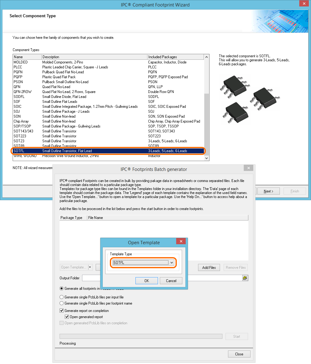
Support for SOTFL packages, added to the IPC-Compliant Footprint Wizard and IPC-Compliant Footprints Batch Generator.
The following tables list the information (required and optional) when defining the SOTFL package in an Excel file for use with the IPC-Compliant Footprints Batch Generator. Similar required information will be reflected in the corresponding pages of the IPC-Compliant Footprint Wizard.
Table of data related to SOTFL Package Specifications.
| Name | Value Required | Format | Description (Dimensions in mm) |
|---|---|---|---|
| FootprintName | Optional | String | If blank, then auto-generated IPC naming will be used |
| FootprintDescription | Optional | String | If blank, then description is auto-generated |
| Dmin, Dmax | Yes | Real | Minimum and maximum body length |
| Emin, Emax | Yes | Real | Minimum and maximum lead span |
| E1min, E1max | Yes | Real | Minimum and maximum body width |
| PinCount | Yes | 3,5 | Total number of pin positions, not including tab |
| PinOrder | Optional | String | Comma separated list showing pin order. If blank pin order is assumed sequential from 1 to PinCount. Example: 8,7,6,5,4,3,2,1 will reverse the pin order of an 8 pin package |
| AbsentPins | Optional | String | Comma separated list showing absent pins. Example: 1,2,5. If blank all pins present |
| Bmin, Bmax | Yes | Real | Minimum and maximum width of narrow leads |
| B1min, B1max | Optional | Real | Minimum and maximum width of wide lead (3 pin packages only) |
| cmin, cmax | Optional | Real | Minimum and maximum lead thickness |
| L1min, L1max | Optional | Real | Minimum and maximum lead length (from body to end of lead) |
| LPmin, LPmax | Yes | Real | Minimum and maximum lead length |
| Pitch | Yes | Real | Pitch (e) |
| Amin, Amax | Yes | Real | Minimum height |
| DensityLevel | Yes | L, M, N | M = Most or maximum copper (density level A), N = Nominal or median copper (density level B), L = Least or minimum copper (density level C) |
| JHmin | Optional | Real | Minimum value for heel fillet |
| JSmin | Optional | Real | Minimum value of side fillet |
| JTmin | Optional | Real | Minimum value for toe fillet |
| DrawingNote | Optional | String | If package has other features that will affect the footprint, then enter details. |
Table of data related to SOTFL Footprint Specifications.
| Name | Value Required | Format | Description (Dimensions in mm) |
|---|---|---|---|
| Z | Optional | Real | Distance between pads. Measured from outside edges |
| C | Optional | Real | Distance between pads. Measured from pad centre |
| G | Optional | Real | Distance between pads. Measured from inside edges |
| X | Optional | Real | Pad width |
| Y | Optional | Real | Pad length |
| X1 | Optional | Real | Pad width (large pad) |
| A | Optional | Real | Assembly width |
| B | Optional | Real | Assembly length |
| V1 | Optional | Real | Courtyard width |
| V2 | Optional | Real | Courtyard length |
| R1 | Optional | Real | Silkscreen width |
| R2 | Optional | Real | Silkscreen length |