Early printed circuit boards were all single sided. To successfully implement all of the connections, jumpers, or wire links, were often used to create another layer of connectivity, which could pass across the printed routing. The image below shows an example of Jumpers being used in Altium Designer to implement the routing on one side of the board.
Note the representation of a Jumper, with a curved connection line between the 2 pads. In the image the jumper connection lines are shown in different colors, that is because they inherit the color assigned to the net.
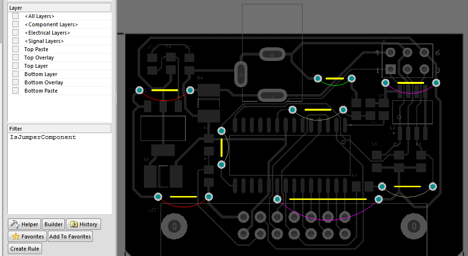
Jumpers allow this design to routed single-sided.
What Defines a Jumper?
To act as a jumper, you need:
- The component Type to be set to Jumper
- Both of the pads in the Jumper component to have their Jumper ID set to the same, non-zero value.

Once the component Type and pad JumperID properties are set, the component behaves as a Jumper.
How Jumpers are Used
How you work with Jumpers is still being finalized. At this stage there is no automatic net inheritance, after placing a Jumper in the workspace you will need to set the Net attribute of one of the pads manually, in the Pad dialog. Note that if the component is defined as a Jumper, then the other pad will automatically inherit the same Net name.
Controlling the Display of Jumpers
The View menu includes a new Jumpers sub-menu, allowing control over the display of Jumper components. There are also sub-menus added in the Netlist popup menu (N shortcut).
The N shortcut now includes options to control the display of Jumper connection lines.
A new query keyword, IsJumperComponent has been added for filtering and rule definition.
Jumpers and the Bill of Materials
Jumpers are typically pieces of tinned copper wire bent to the correct length. That means they need to be in the BOM. To support this, Jumpers can also be included on the schematic so that they are included into the Bill of Materials. The Synchronizer and the Report engine have the following behavior for synchronizing Jumpers:
- The component itself is synchronized
- Net properties of Jumper pins are not synchronized
- The Jumper is included in the BOM
Suggested Workflow for Working with Jumpers
The following description is one approach to working with Jumper components. This workflow starts at the schematic, but you can also start by placing the Jumper footprints directly onto the PCB. The main reason for starting on the schematic is that when the design is transferred to the PCB workspace, the footprints will have the correct component Type of Jumper. If you place them directly from the PCB library into the PCB workspace, the component Type will default to Standard, so you will need to manually set this.
Create the Jumper Footprints in the PCB Library
Create a footprint for each length jumper that will be used. Typically jumpers are designed in pre-defined lengths, for example in increments of 0.1 inch (100 mils).
As mentioned above, there are 2 conditions that make a Jumper a Jumper,
- Both pads in the Jumper must have their Jumper ID set to the same, non-zero value. Note that it does not matter if the pads in all Jumper footprints used on a board design have the same Jumper ID value.
- The Jumper Component must have its Type set to
Jumper. Note that this can only be set once the footprint has been placed into the PCB workspace, it cannot be set in the PCB Library editor.
The image below shows a typical Jumper in the PCB Library editor. Both pads have the Jumper ID = 1.
A simple Jumper footprint, this one is for a 200 mil long Jumper.
Create the Schematic Jumper Component
On the schematic side, you can either:
- Create a single Jumper component, then add all of the different length Jumper footprints that you need to it.
- Create an individual Jumper component for each different length Jumper footprint that will be used.
In this Workflow the first approach is used.
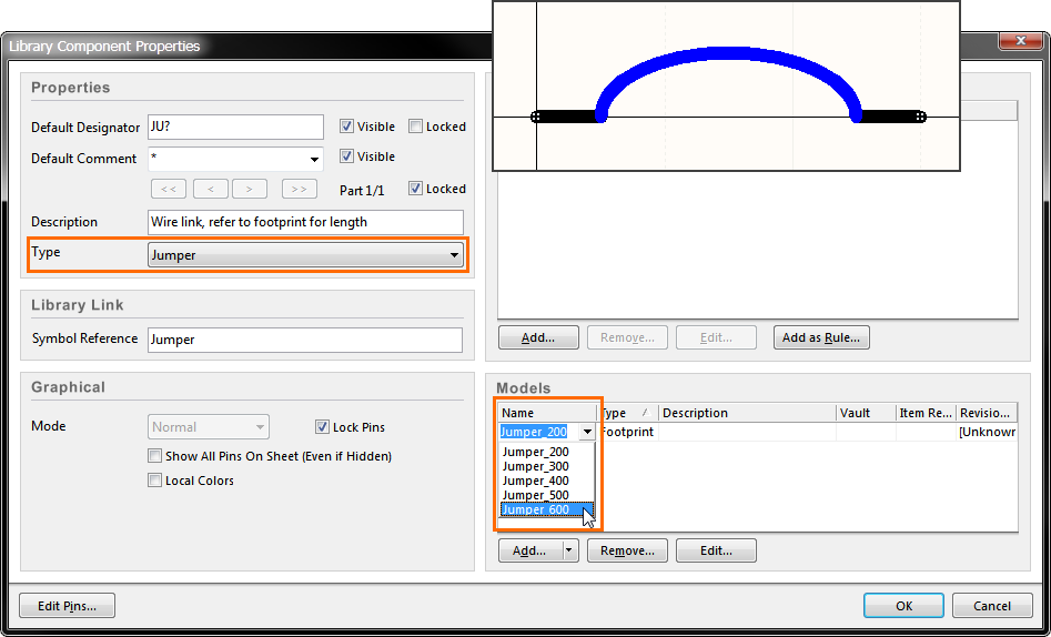
The symbol has been created, the footprints added, the Type set to Jumper, and the Default Designator and Description defined.
Once the symbol has been created, you:
- Set the default Designator, in this example it is JU?
- Set the Component Type to
Jumper - Add the various Jumper footprints to the Models list, as shown in the image above
- Define the other component properties you need, such as the Description and any required component Parameters.
Placing Jumpers onto the Schematic
Once the Jumper has been designed, you can place a number of them onto the schematic. At this stage you probably do not know how many you will need, but extras can easily be deleted. Keep in mind they are on the schematic to ensure they go into the BOM, they do not need to be wired into the circuit at each location they end up being used. For that reason it makes sense to place them all on the same schematic sheet, perhaps with other BOM-only hardware, such as screws.
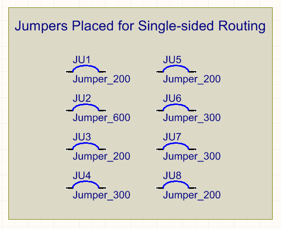
Jumpers have been placed on a schematic sheet, this image was taken once the entire process was completed.
When a Design » Update PCB is performed, all of the jumpers will be placed into the PCB workspace using the default footprint, to the right of the board shape.
Position and Routing the Jumpers on the PCB
The image below shows the PCB, almost completely routed, note the remaining connection lines showing where the routes are not complete. There are also a number of un-placed Jumper components to the right of the board.
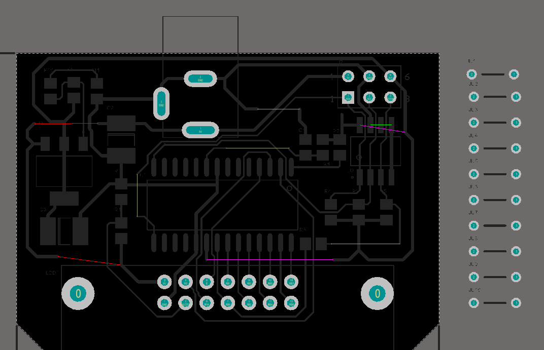
This board has been routed as much as possible, the connection lines show the remaining, unrouted connections.
The routing for each of these connections can not be completed because there is no route path available on this single-sided design. To complete them, the Jumper components will be used.
To complete a connection with a Jumper:
- Drag a jumper component into position on the board. If it is not long enough, either press Tab while moving the Jumper, or double-click once it is placed, to open the Component dialog.
- In the Footprint Name field of the Component dialog, type in the required footprint name, or click the button and select the required footprint.
- To make it easier to include the Jumper in the BOM, enter a suitable identifying string in the Comment field of the Component dialog. In the image below the footprint name has been copied and pasted into the Comment field, since it describes how long the jumper is.
- Position the Jumper in the required location.
- Double-click to edit one of the pads, and select the required net name from the Net dropdown list. The other pad in the Jumper will automatically be assigned the same net name.
- Once all Jumpers have been placed, delete any unused Jumpers from beside the board.
- Now run the Design » Update Schematic command to push the footprint and comment changes back to the schematic.
- The last step is to remove any unused Jumper components from the schematic. These can be identified by switching to one of the schematic sheets and running the Design » Update PCB command. The ECO dialog will list any extra components on the schematic; note their designators, Close the ECO dialog, then delete those excess Jumpers from the schematic. An example of Jumpers on a schematic sheet are shown in an image earlier in this article.
The animation shows the process of placing and configuring a Jumper component.