Old Content - visit altium.com/documentation
Related Videos
Enhanced design rules give the designer greater control over the board design process. Altium Designer 14.3 includes a new design rule, SMD Entry. This rule controls how the routing is allowed to enter an SMD pad, along with the default entry point of the end of the pad, the designer can also choose to allow the following entry points:
- Corner - allow the track to enter through the corner of the pad
- Side - allow the track to enter the side of the pad (the longer edge), at 90 degrees. Note that the side must be more that twice the length of the end for this option to be applied. If not then all edges are treated as an end of the pad.
- Any Angle - allow the track to enter the pad at any angle, at any location around the edge of the pad.
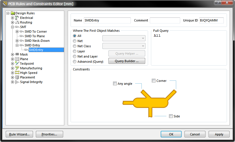
Use the SMD Entry design rule to control how the routing enters an SMD pad.
Note that:
- The rule applies to surface mount pads only, that is, a pad defined on a single copper layer.
- The end of the pad is determined from the pad dimensions, the ends are the shorter edges.
- Pads can always be entered from either end (the shorter edge)
- The rule is applied on both routing out of the pad (exit) and into the pad (entry).
- The rule works in harmony with the SMD To Corner design rule, configure both to ensure neat SMD routing.