Contents
- Fills and Solid Regions
- Polygon Pours
- Placing a Polygon Pour
- Polygon Fill Mode
- The Placement Process
- Corner Modes
- Understanding the Look-Ahead Feature
- Connecting the Polygon to a Net
- Remove Dead Copper
- Controlling the Polygon Connection Style
- Controlling the Polygon Clearance
- Re-pouring a Polygon
- Polygon Cutouts
- Creating a Polygon Pour From a Set of Tracks
- Moving a Polygon Pour
- Reshaping a Polygon Pour
- Slicing a Polygon Pour
- Shelving a Polygon Pour
- Using Polygon Pours on Non-copper Layers
- The Polygon Pour Manager
- Reporting on Polygons
- Using the List Panel to View and Edit Polygon Properties
A common requirement on a printed circuit board is large areas of copper. It could be a hatched region of grounding copper on an analog design; a large, solid region of copper for carrying heavy power supply currents; or a solid ground area for EMC shielding. In Altium Designer areas of copper can be defined using three different design objects: Fills, Solid Regions and Polygon Pours. The advantage of a Polygon Pour is that it automatically pour around copper objects that belong to another net, in accordance with the applicable Electrical Clearance and Polygon Connect Style Design Rules.
This article briefly discusses Fills and Solid Regions, and then explains how Polygon Pours (also called copper pours) are used to create regions of copper on a PCB. It covers such topics as placing and modifying Polygon Pours, setting properties, controlling the clearance using design rules and repouring.
Fills and Solid Regions
A example of a Solid Region, that is selected.
A Fill (Place » Fill) is a rectangular shaped design object that can be placed on any layer, including copper (signal) layers. Fills are limited to a rectangular shape and will not avoid around other objects, such as Pads, Vias, Tracks, Regions, other Fills or Text. If a Fill is placed on a signal layer it can be connected to a Net.
A Region (Place » Solid Region) is a design object used for defining polygonal shapes. A Solid Region (commonly just called Region) can be placed on any layer, including signal (copper) layers. Like a Fill, a Region does not avoid around other objects, such as Pads, Vias, Tracks, Fills, other Regions or Text. If a Region is placed on a signal layer it can be connected to a Net.
The Region object also has a number of special properties that allow it to be used for:
- Polygon cutouts - where it is essentially a negative (empty) object that the surrounding Polygon pours around.
- Board Shape cutouts - where it also acts as a a negative (empty) object to define an irregular cutout or hole in the board.
- Custom Pad shapes - where it defines the copper area of an unusual pad, giving the ability to define automatically matched-shape solder and paste mask contractions/expansions.
Polygon Pours
A Polygon shown as solid and hatched, demonstrating varying clearances and controlled connection style and air gap.
A Polygon Pour (Place » Polygon Pour) placed on a signal layer creates a polygonal (multi-sided) area of copper, which can either be solid or hatched. As they are poured, Polygons automatically allow for clearances around electrical objects belonging to a different net, connect to objects of the same net, and fill irregularly shaped areas. Clearances and connection properties are controlled by the applicable Electrical Clearance and Polygon Connection Style design rules.
Placing a Polygon Pour
Select the Place » Polygon Pour command to place a Polygon on the current layer in the PCB Editor. When the command is run the Polygon Pour dialog displays, where you set the fill and net connection options and pour-around properties. Click OK and the cursor changes to a crosshair, ready to draw the Polygon outline.
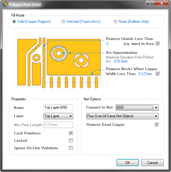
The Polygon Pour dialog, where you configure the properties of the polygon before placing it.
When you place a Polygon, you are defining the outline of the Polygon object. Once the outline is complete, the polygon will automatically fill, in accordance with the Fill Mode and other options selected in the dialog.
Polygon Fill Mode
There are 3 supported Fill Modes, Solid, Hatched or None.
Solid (Copper Regions) - If this mode is selected the Polygon is internally constructed from Solid Region objects, with a separate Region for each contiguous area of copper in the completed polygon. This type of polygon is output to Gerber using Gerber region definitions. Note that circular cutouts are not supported in the Gerber region definition, so the arcs (holes) for circular cutouts are actually approximated by straight chord sections. The accuracy of these is defined by the Arc Approximation setting in the Polygon Pour dialog. Polygons of this type are generally faster to pour and result in smaller PCB and Gerber file sizes.
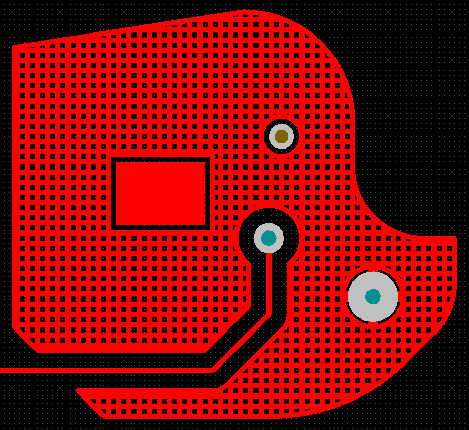
Hatched (Tracks/Arcs) - If this mode is selected the polygon is created from Track and Arc objects. By adjusting the Width and Grid settings of the Track/Arc objects, the completed polygon can either be hatched or solid in appearance. Polygons of this type are generally slower to pour and result in larger PCB and Gerber file sizes. Hatched polygons are often used in analog designs. Note that the outline of a Hatched polygon is created from Tracks and Arcs, with the user-defined edge of the Polygon at the center-line of the outline Tracks and Arcs.
None (Outlines Only) - this mode is essentially the same as the Hatched mode. It also uses Tracks and Arcs to define the boundaries, but the fill-in Tracks and Arcs are not added. This mode can be useful if you are analyzing the structure and design of various polygons and attempting to understand the interaction of overlapping polygons. This mode is also useful when design changes are being made and the polygon is interfering in this process. An alternate approach to using outlines during design changes is to Shelve the polygons, where they are retained in the PCB file, but removed from view.
The Placement Process
In Altium Designer's PCB Editor the process of how you define any multi-sided polygonal object, such as a Solid Region, the Board Shape or a Polygon, is the same. Solid objects are closed objects, so regardless of how far you are through the placement process, the software will show a line from the cursor back to the object's starting location. This line will become the solid object's last edge if you press Escape (or right-mouse click) to terminate the placement process. The placement process is a process of defining the corner locations, with various corner modes being available.
Corner Modes
There are 5 different corner modes available during polygon placement: 45º, 45º arc, 90º, 90º arc and Any Angle, as shown in the images below (click to enlarge).

The different corner modes available during polygon placement, press Shift+Spacebar to cycle through the modes.
Tips on Placing a Polygon:
- Press Shift+Spacebar to cycle through the corner modes
- Press Spacebar within each corner mode to toggle the corner direction (except for the Any Angle mode).
- Press Backspace to remove the last corner.
- Press Esc or Right-Mouse click to terminate the placement process, the software will close and complete the Polygon.
- For the Arc corner modes, the arc can be re-sized using the
 and keys. Hold Shift to accelerate the re-sizing process.
Understanding the Look-Ahead Feature
There are many situations during PCB design where the designer needs to be able to predict where a future track segment or object edge must go, without committing to place that object. To support this requirement Altium Designer includes a feature called Look-Ahead. When Look-Ahead is enabled the track/object edge currently attached to the cursor is not placed when the designer clicks, only the previous segment is placed. To say that another way, the last segment allows the designer to look-ahead to where they will place the future segment.
Press the 1 shortcut during object placement to toggle Look-Ahead on or off, note how the display changes to display each mode. In track placement, the segments to be placed by the next mouse click are shown as hatched, and the Look-Ahead segment is shown as hollow or empty. In solid-object placement, the edges to be placed by the next mouse click are shown as solid white lines and the Look-Ahead edge is shown as a dashed white line.
The following images shows how the display of track segment changes when the Look-Ahead feature is on and off.
Track placement with Look-Ahead on (left image) and off (right image). The next mouse click will place the hatched track segments.
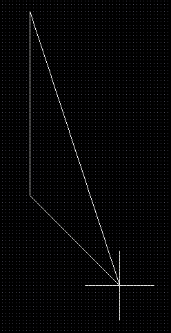
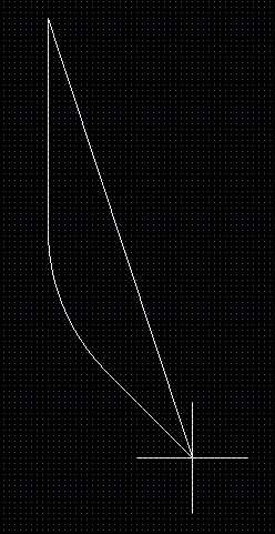
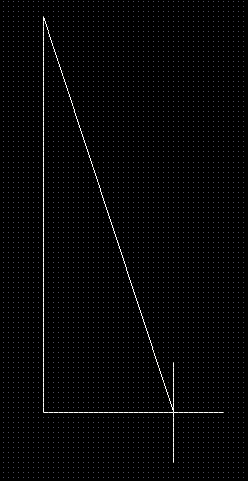
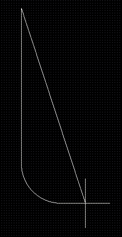
The Look-Ahead feature also works during Polygon Pour placement, press the 1 shortcut (during object placement) to toggle it on and off. The following images show the first corner placement of a Polygon Pour, first with Look-Ahead on, then with Look-Ahead off.
Look_ahead is on, on the next mouse click the solid line becomes a polygon edge, but not the dotted line. Note the solid return line, it shows how the polygon will be closed if the designer terminates polygon placement.
Look_ahead is off, on the next mouse click both of the solid lines becomes polygon edges. Note the solid return line, it shows how the polygon will be closed if the designer terminates polygon placement.
Connecting the Polygon to a Net
A Polygon can be attached to a net. Select the required net in the Connect to Net drop-down in the Polygon Pour dialog. The Polygon pour will connect to each pad on this net that is found within the outline of the Polygon. How the polygon connects to the pads is determined by the applicable Polygon Connect Style design rule. The clearance between the polygon and objects belonging to other nets is determined by the applicable Electrical Clearance design rule.
How the polygon treats objects on the same net, such as routing tracks, is determined by the option selected in the Pour Over drop-down:
- Pour Over All Same Net Objects - choose this option if you want the Polygon to automatically connect to all objects on the same net as the pour.
- Pour Over Same Net Polygons Only - choose this option (default) if you want the Polygon to automatically connect to only Polygon objects inside its boundary, which are attached to the same net.
- Don't Pour Over Same Net Objects - choose this option if you specifically do not wish the Polygon pour to connect to any other, non-pad objects on this (or any other) net.
Remove Dead Copper
When a polygon is poured there can be regions (islands) of the polygon that are completely isolated from the connected net, due to the presence of other tracks, pads and so on. To have the software detect and remove these isolated islands of copper, enable the Remove Dead Copper option.
Controlling the Polygon Connection Style
Main article: Polygon Connect Style Design Rule
How the polygon connects to pads on the net that it is attached to, is controlled by the applicable Plane - Polygon Connect Style design rule (Design » Rules).
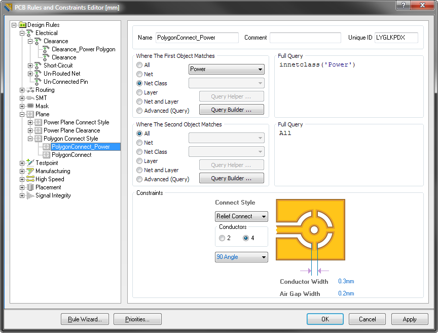
How the polygon connects to pads on the net is determined by the Polygon Connect Style design rule.
Three connection options are available:
- Direct Connect - the polygon effectively pours over the pad, creating solid copper to the pin.
- Relief Connect - A spoke-style connection is created: define the Number of conductors, the Angle of these conductors (90º or 45º), Conductor Width,and the Air Gap Width ** (the clearance between the edge of the pad and the edge of the polygon surrounding the pad).
- No Connect - the pads on the net will be isolated from the polygon.
Controlling the Polygon Clearance
Like any object placed on a signal (copper) layer, the clearance of a polygon from objects that it is poured around is controlled by the applicable Electrical Clearance design rule.
![]()
The clearance from the Polygon to objects on other nets is controlled by the Electrical Clearance design rule.
It is common practice to have a larger clearance between a polygon and other net objects, to achieve this a polygon-specific Electrical Clearance design rules can be defined. An example of this is shown in the image above (click to enlarge), where the rule states that:
Objects that are InPolygon, and belong to a Net Class called Power
and
All other copper objects
Must be at least 0.3 mm apart.
In this example the designer is targeting only the Polygons attached to power nets, which require a greater clearance than other non-power net Polygons. Remember that the Polygon Clearance rule must also have a higher Priority than any general clearance rule to have any effect.
Re-pouring a Polygon
There are a number of ways a Polygon can be re-poured.
To repour a Polygon:
- Double click anywhere on the Polygon to open the Polygon Pour dialog, change settings as required and click OK.
- Right-click on the Polygon, then in the floating Context menu select Polygon Actions » Repour.
- In the Polygon Manager (Tools » Polygon Pours » Polygon Manager), select the required Polygon, then click the Repour button.
- Use the appropriate Repour command in the Tools » Polygon Pours sub-menu.
Confirm the repour by clicking Yes in the Confirm dialog.
Polygon Cutouts
A Polygon Pour Cutout is essentially a negative copper region, that is the designer is defining a void or hole in the Polygon. To define a cutout in a Polygon select the Place » Polygon Pour Cutout command, then click to define the cutout shape. Once the cutout has been defined the Polygon must be re-poured, it will then pour around the cutout definition. Remember that the cutout is actually a Solid Region object, it can be re-sized by clicking once to select it, then clicking and holding to drag an edge or a vertex. After re-sizing the cutout the polygon must be re-poured.
The cutout has been placed (left image), and the Polygon has been re-poured (right image).
Creating a Polygon Pour From a Set of Tracks
As well as defining areas of electrical copper on a board, Polygons and Solid Regions are also used to define other polygonal-shaped design objects, such as a special symbol or a company logo. If an outline of the required shape has been defined in another design tool, such as AutoCAD, it can be exported as DXF and then imported into Altium Designer. That outline can then be converted into a Polygon or a Solid Region.
To convert a set of tracks to a polygon, select the track segments and then select Tools » Convert » Create Polygon from Selected Primitives from the menus.
Note that:
- The Polygon will be created on the current (or active) layer, not the layer that the selected tracks are on. This means you can define the shape on a Mechanical Layer, then create the polygon on a signal layer.
- The selected tracks will still exist after polygon has been created, and will remain selected.
- If the polygon is created on the same layer as the selected tracks it will pour within the tracks, in accordance with the applicable Electrical Clearance Design Rule.
- The Polygon will be created with its Fill Mode set to None (Outline Only), double click on it to re-pour it with the required Fill Mode.
Moving a Polygon Pour
Click and drag to move a Polygon pour. Hold down the SHIFT key to select multiple Polygon pours to move. The rebuild Confirm dialog appears when you release the mouse button. Click Yes to repour the Polygon pour(s) in their new location.
Reshaping a Polygon Pour
A Polygon, with 90º arc corners, being re-sized.
An existing Polygon pour can be reshaped. To do this, first right-click on the polygon and select Polygon Actions » Move Vertices (or Edit » Move » Polygon Vertices). The following actions can then be performed:
- Position the mouse cursor over an edge, click to select the edge, slide that edge to a new location, then click to place it.
- Click to select a vertex, move that vertex to a new location, then click to place it. If you select a vertex at the center of a straight edge this will in effect break that single edge into 2 new edges.
- To remove a vertex, click to select and move it, then press the Delete key on the keyboard. The software will remove that vertex, then automatically move the next vertex in an anti-clockwise direction to the cursor. The visual effect is that it appears to remove not the current vertex, but the next one in an anti-clockwise direction.
- Right-click to terminate reshaping, then click Yes in the Confirm dialog to re-pour the Polygon in the new shape.
Slicing a Polygon Pour
The Place » Slice Polygon Pour command is used to slice a single Polygon pour into two or more separate Polygon pours. When you select the command you are in slice mode (similar to track placement mode), click (or press ENTER ) to anchor a series of vertex points that define the slice line. When defining the slice, press Shift+Spacebar to cycle through the corner modes, press the Spacebar to toggle between the Start and End corner modes and use the Backspace key to remove the last placed corner. Place the end of the slice beyond the edge of the Polygon. When you have finished defining the slice, right-click (or press ESC).
A confirmation dialog appears stating how many new Polygons will be created. Click Yes and confirm that you wish to rebuild the Polygons.
Shelving a Polygon Pour
During the design process it is normal for changes to occur - components might be added or change, routing may need to be updated. To simplify the management of existing Polygons during this process, they can be Shelved. This temporarily hides them from the editor, but retains them in the PCB database.
- To shelve all Polygon pours in the current design, select the Tools » Polygon Pours » Shelve n Polygon(s) command (where n is the number of Polygon pours that have been detected in the design).
- To restore all shelved Polygon pours, select the Tools » Polygon Pours » Restore n Shelved Polygon(s) command (where n is the number of Polygon pours that are currently shelved).
- You can also selectively shelve via the right-click menus command, or the Polygon Manager.
Using Polygon Pours on Non-copper Layers
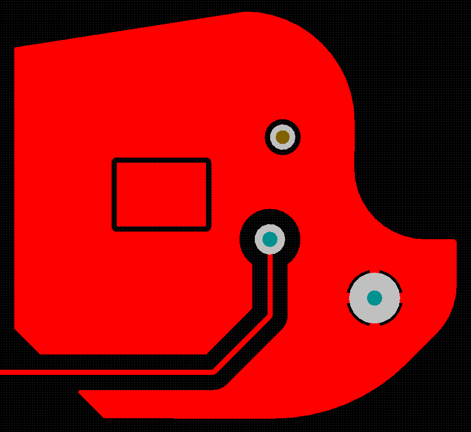
Polygon pours can be used on non-copper layers. If a Polygon pour is placed on a non-signal layer, it will not pour around existing objects because they are not assigned to a net.
The Polygon Pour Manager
Main article: Polygon Pour Manager
The Polygon Pour Manager dialog provides a high-level view of all Polygons that currently exist in the PCB workspace. This manager also allows you to name and rename each Polygon, set the pour order of Polygons, perform re-pouring or shelving actions on selected Polygons and add/scope design rules for selected Polygons as well.
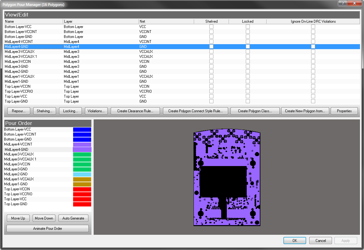
The Polygon Manager gives full control over all the Polygons in the design.
Notes about the Polygon Pour Manager:
- The Polygon Pour Manager dialog is launched from the Tools » Polygon Pours submenu.
- A Polygon is automatically named during placement, you are free to rename it to suit your design. Note that the Name can be used to scope design Rules targeting a Polygon Polygon.
- The Pour Order section at the bottom of this dialog allows you to re-arrange the pour order of Polygons with the Move Up , Move Down , and Auto Generate buttons. You can also change order using mouse drag-and-drop functionality, which is far more expedient in designs featuring many polygon pours.
- Pour order can be important when there is a Polygon completely enclosed within another Polygon, typically you would order from the smallest Polygon down to the largest Polygon.
- The Auto Generate button will order the Polygons from smallest area to largest area, on a layer-by-layer basis.
- Since the Polygon manager can perform actions that change the design, such as repouring selected Polygons, it must execute pending actions before accepting a new request that can change the design. A message alerting you about this will appear (shown below).
- If you click the Repour button you have the choice of re-pouring all Polygons, selected Polygons or Polygons that have violations. Update progress can be monitored on Altium Designer's status bar.
- If you perform a Shelve, Lock, or Ignore from DRC action for selected Polygons the action is not performed immediately. In these cases the actions are performed when you click the Apply or OK buttons.
Any pending edits must be applied before a new edit can be performed.
Reporting on Polygons
For more information about the Polygon pours in your PCB, you can use the Board Information Report or list the properties of a Polygon pour and its children. Select Reports » Board Information. The number of Polygons detected on the PCB is shown in the PCB Information dialog. Keep in mind that this total reflects not only Polygon pours, but also internal planes and split planes. For a detailed listing of Polygon properties, use the PCB List panel.
Using the List Panel to View and Edit Polygon Properties
Main article: PCB List
The PCB List panel provides an alternate approach to view and edit all design objects that currently exist in the workspace. To display the PCB List panel click the PCB button down the bottom right of the workspace, then select PCB List from the menu. The PCB List panel presents data in a tabular, or spreadsheet-like format. By default it will display all objects in the workspace. Use the controls across the top of the panel to filter down the list, in the image below you can see that the PCB List panel is set to Edit, All Objects, only of kind Polygon (click to enlarge). The properties of one or more polygons can be edited in the PCB List panel.
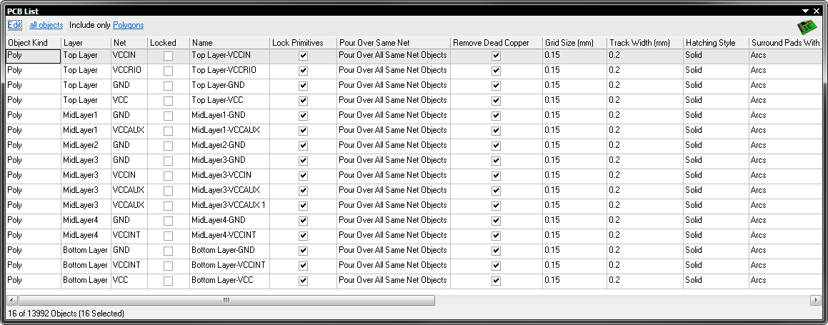
The PCB List panel can be used to review and edit Polygon pours.