Contents
- What is Rigid-Flex?
- Rigid-Flex Design
- Materials Used in Flexible Circuit Manufacture
- Flex and Rigid-Flex Layer Stackup Types
- Type 1 - Single Layer
- Type 2 - Double Layer
- Type 3 - Multilayer
- Type 4 - Multilayer Rigid-Flex
- How Rigid-flex is Supported in Altium Designer
- Multiple Layer Stacks
- The Board Shape
- Assigning a Layer Stack to a Region of the Board
- Placing and Managing Flex Bend Lines
- Design Considerations
- Documentation and Drawing Requirements
- Additional Drawing Detail
- References

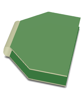
A rigid-flex circuit, designed to tightly integrate into its enclosure.
What is Rigid-Flex?
As the name suggests, a flexible printed circuit is a pattern of conductors printed onto a flexible insulating film. Rigid-flex is the name given to a printed circuit that is a combination of both flexible circuit(s) and rigid circuit(s), as shown in the image above. This combination is ideal for exploiting the benefits of both flexible and rigid circuits - the rigid circuits can carry all or the bulk of the components, with the flexible sections acting as interconnections between the rigid sections.
Flexible circuit technology was initially developed for the space program to save space and weight. They are popular today as they not only save space and weight - making them ideal for portable devices such as mobile phones and tablets - they can also: reduce packaging complexity by substantially reducing the need for interconnect wiring; improve product reliability due to reduced interconnection hardware and improved assembly yields; and reduce cost, when considered as part of the overall product manufacture and assembly costs.
Flexible circuits are normally divided into 2 usage classes: static flexible circuits, and dynamic flexible circuits. Static flexible circuits (also referred to as use A) are those that undergo minimal flexing, typically during assembly and service. Dynamic flexible circuits (also referred to as use B) are those that are designed for frequent flexing; such as a disk drive head, a printer head, or as part of the hinge in a laptop screen. This distinction is important as it affects both the material selection and the construction methodology. There is a number of layer stack-up configurations that can be fabricated as rigid-flex, each with their own electrical, physical and cost advantages.
Rigid-Flex Design
Designing a flex or rigid-flex circuit is very much an electromechanical process. Designing any PCB is a 3 dimensional design process, but for a flex or rigid-flex design the 3 dimensional requirements are much more important. Why, because the rigid-flex board may attach to multiple surfaces within the product enclosure, and this attachment will probably happen as part of the product assembly process. To ensure that all sections of the finished board fit in their folded location within the enclosure, it is strongly recommended that a mechanical mock up (also known as a paper doll cut out) is created. This process must be as accurate and realistic as possible with all possible mechanical and hardware elements included, and both the assembly-time phase and the finished assembly must be carefully analyzed.
Materials Used in Flexible Circuit Manufacture
Flex circuits are created from a stackup of flexible substrate material and copper, laminated together with adhesive, heat and pressure.
The most common substrate is polyimide, a strong, yet flexible thermosetting polymer (thermoset). Examples of polyimides often used in the manufacture of flexible circuits include: Apical, Kapton, UPILEX, VTEC PI, Norton TH and Kaptrex. Note that these are registered trade names, owned by their respective trademark holders.
The copper layer is typically rolled and annealed (RA) copper, or sometimes wrought copper. These forms of copper are produced as a foil and offer excellent flexibility. They have an elongated grain, it is important to orient this correctly in a dynamic flex circuit to achieve the maximum flexing lifespan. This is achieved by orienting the dynamic flex circuit along the roll (so the circuit bends in the same way the foil was coiled on the roll). The flex manufacturer normally deals with this during the preparation of fabrication panels, it only becomes an issue if the designer performs their own circuit panelization (referred to as nesting in flex circuit design). The copper foil is typically coated with a photo-sensitive layer, which is then exposed and etched to give the desired pattern of conductors and termination pads.
The adhesive is typically acrylic, and as the softest material in the structure, introduces the greatest number of manufacturing challenges. These include: squeeze-out, where the adhesive is squeezed out into openings cut into the cover layers to access copper layers; Z-axis expansion defects due to the higher CTE (coefficient of thermal expansion) of acrylic adhesive; and moisture out gassing due to the higher rate of moisture absorbance, which can result in resin recession, blow outs and delamination at plated through hole sites. Alternative adhesives and adhesive-less processes are available, these may be more appropriate in less cost-sensitive applications.


A simplified view of how a flexible circuit is manufactured, the materials are laminated together under heat and pressure.
Flex and Rigid-Flex Layer Stackup Types
There are a number of standard stackups available for flex and rigid-flex circuits, referred to as Types. These are summarized below.
Type 1 - Single Layer
Single-sided flexible wiring containing one conductive layer and one or two polyimide outer cover layers.
- One conductive layer, either laminated between two insulating layers or uncovered on one side.
- Access holes to conductors can be on either one or both sides.
- No plating in component holes.
- Components, stiffeners, pins and connectors can be used.
- Suitable for static and dynamic flex applications.

A Type 1 flex structure with 2 cover layers, access holes on both sides and no plating in the in the component holes.
Type 2 - Double Layer
Double-sided flexible printed wiring containing two conductive layers with plated through holes, with or without stiffeners.
- Two conductive layers with an insulating layer between; outer layers can have covers or exposed pads.
- Plated through-holes provide connection between layers.
- Access holes or exposed pads without covers can be on either or both sides; vias can be covered on both sides.
- Components, stiffeners, pins and connectors can be used.
- Suitable for static and dynamic flex applications.


A Type 2 flex structure with access holes on both sides and plated through holes.
Type 3 - Multilayer
Multilayer flexible printed wiring containing three or more conductive layers with plated-through holes, with or without stiffeners.
- Three or more flexible conductive layers with flexible insulating layers between each one; outer layers can have covers or exposed pads.
- Plated through-holes provide connection between layers.
- Access holes or exposed pads without covers can be on either or both sides.
- Vias can be blind or buried.
- Components, stiffeners, pins and connectors can be used.
- Typically used for static flex applications.

A Type 3 flex structure with access holes on both sides and plated through holes.
Type 4 - Multilayer Rigid-Flex
Multilayer rigid and flexible material combinations (Rigid-Flex) containing three or more conductive layers with plated-through holes. Rigid-flex has conductors on the rigid layers, which differentiates it from multilayer circuits with stiffeners.
- Two or more conductive layers with either flexible or rigid insulation material as insulators between each one; outer layers can have covers or exposed pads.
- Plated through-holes extend through both rigid and flexible layers (apart from blind and buried vias).
- Access holes or exposed pads without covers can be on either or both sides.
- Vias or interconnects can be fully covered for maximum insulation.
- Components, stiffeners, pins, connectors, heat sinks, and mounting brackets can be used.


A Type 4 rigid-flex structure, the rigid sections are formed by adding rigid layers to the outside of the flex structure.
How Rigid-flex is Supported in Altium Designer
Altium Designer's PCB editor is a layered design environment, supporting up to 32 signal layers and 16 plane layers. These copper layers are separated by insulation layers. In a traditional rigid PCB these insulating layers are typically fabricated using FR4 and pre-preg, although there is a range of materials available, each with properties that suit different applications. For a traditional rigid PCB these copper and insulating layers exist across the entire PCB, so a single layer stack can be defined for the entire board area.
The layer stack for an eight layer rigid circuit, as it was configured in earlier versions of Altium Designer.
A rigid-flex design does not have a consistent set of layers across the entire circuit design, the rigid section of the board will have a different set of layers from the flexible section. And if the rigid-flex design has a number of rigid sections joined by a number of flex sections, then there may be a different set of layers used in each of these sections. A PCB editor with a single layer stack cannot support this design requirement. To support this, Altium Designer's layer stack management system has been enhanced to support the definition of multiple stacks, as shown below.
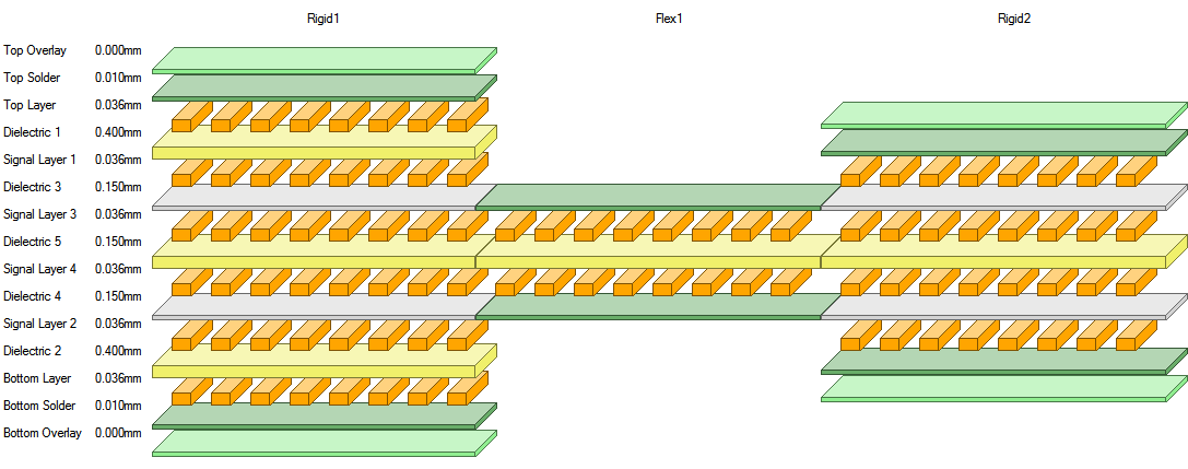
The Layer Stack Manager supports the definition of any number of layer stacks.
Multiple Layer Stacks
Main article: PCB Layer Stack Management
To support the need to define a different set of layers in different areas of the board design, Altium Designer supports the concept of multiple layer stacks. This is achieved by having an overall master layer stack that defines the total set of layers available to the board designer in this design. From this master layer stack, any number of sub-stacks can be defined, using any of the layers available in the master stack. Each sub-stack is defined and named, ready for use in the rigid-flex design.
The Board Shape
Main Articles: Creating and Modifying the Board Shape, Defining Board Regions and Bending Lines
The layer stack defines the board design space in the vertical direction, or Z plane. In Altium Designer, the board space is defined in the X and Y planes by the Board Shape. The board shape is a polygonal region of any shape, with straight or curved edges that lie at any angle, which can also include cutouts (internal holes) of any shape. The board shape is a fundamental concept in Altium Designer's PCB editor, it defines the area available for design - where the components and routing can be placed - and all of Altium Designer's intelligent analysis engines, such as the design rule checker or the autorouter, operate with the boundaries of the board shape.
Note that there is a single, overall board shape for the entire circuit design, including rigid-flex. Within this board shape, any number of board regions can be defined by placing Split Lines to divide the board into separate regions. The image below shows a board shape that has been divided into 3 regions, by the placement of the 2 horizontal blue Split Lines. Use the links above to learn more about splitting a board into multiple regions.
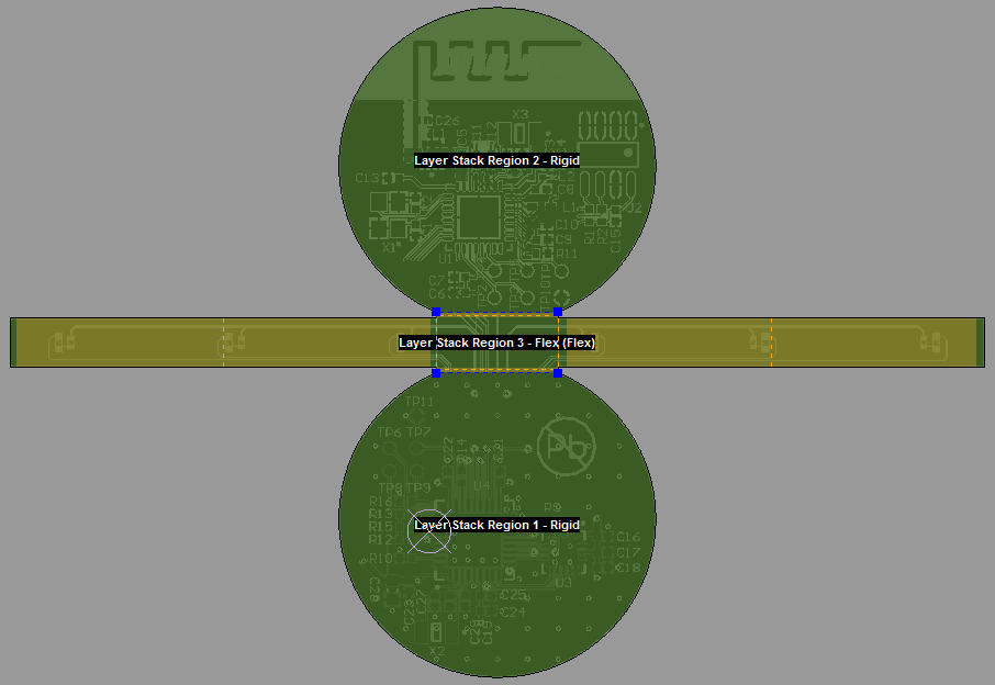
An unusual board shape, note the horizontal dashed blue Split lines, these divide the board into 3 separate regions.
Assigning a Layer Stack to a Region of the Board
Main Article: Defining Board Regions and Bending Lines
As mentioned, in a traditional rigid PCB the copper and insulating layers exist across the entire PCB, so a single layer stack can be defined for the entire board shape. For a rigid-flex design made up of a number of rigid and flex regions, where each region needs a different layer stack, an alternative approach is needed. In Altium Designer this is achieved by supporting the ability to assign a layer sub-stack to a specific region of the board shape. To do this, double click on the region to open the Board Region dialog, then select the required Layer stack in the dropdown, as shown in the image below.
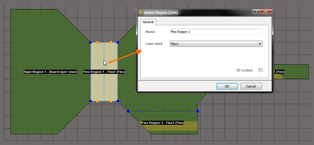
Double-click on a region to open the Board Region dialog and assign the required layer stack.
Placing and Managing Flex Bend Lines
Main article: Defining Board Regions and Bending Lines
If a region has a layer stack assigned, and that stack has the Flex option enabled, then Bending Lines can be placed across that region. Each Bending Line has a: Radius, Bend Angle and an Affected Area Width property, allowing them to be displayed in their folded state, as they would be in a real-world situation.

2 Bending Lines have been defined, allowing this rigid-flex board to be displayed in its folded state.
Design Considerations
- Conductor routing - corners
- Pad shape and area - filleting, rabbit ears (anchoring spurs) for single sided flex,
- Cover layer - avoid stress risers (exposing the incoming track), reduce opening in coverlayer 250um
- Planes
- Staggered length - bookbinding
- service loops
- Conserving copper
- panelization - importance of orientation for flex regions to suit grain of material
- tear resistance - curved corners, drilled hole at corner, hole in slit, leave metal in corners,
- In a flex zone - avoid through holes, route traces at 90 degrees, stagger traces on 2-layer boards (avoid I beaming), material grain to be at right-angles to flex bend, largest possible bend radius, smallest possible flexural arc (total angle of flexure), widen traces through bending zone (especially important for permanent bends)
- The static bend ratio is the ratio of the bend radius to circuit thickness. Ideally, multilayer circuits should have a bend ratio of at least 20:1. For double-sided circuits, the minimum ratio should be at least 10:1. And for single-layer circuits, the minimum ratio should also be at least 10:1
- plated copper is not suitable for flexible circuits,
Documentation and Drawing Requirements
Typical documentation requirements include:
- The Flex PCB shall be fabricated to IPC-6013, class (your requirement here) standards.
- The Flex PCB shall be constructed to meet a minimum flammability rating of V-0 (if required).
- The Flex PCB shall be RoHS compliant (if required)
- The rigid material shall be GFN per IPC-4101/24 (if using epoxy material)
- The rigid material shall be GIN per IPC-4101/40 (if using polyimide material)
- The flexible copper clad material shall be IPC 4204/11 (flexible adhesiveless copper clad dielectric material)
- The covercoat material shall be per IPC 4203/1.
- The maximum board thickness shall not exceed (your requirement here) and applies after all lamination and plating processes. This is measured over finished plated surfaces.
- The thickness of acrylic adhesive through the rigid portion of the panel shall not exceed 10 % of the overall construction. See comments on this above.
- Pouch material can be used for ease of manufacturing and must be removed from the flexible portion of the board prior to shipping.
- The flexible section thickness shall be (your requirement here, do not add this note if this thickness is not critical).
- Minimum copper wall thickness of plated through holes to be (your requirement here) {.001” average is recommended} with a minimum annular ring of (your requirement here). (.002 is recommended)
- Apply green LPI soldermask (if required) over bare copper on both sides, in the rigid sections only, of the board. All exposed metal will be (your surface finish requirement here).
- Silkscreen both sides of the board (if required) using white or yellow (most common) non-conductive epoxy ink.
- Your marking and identification requirements here.
- Your electrical test requirements here.
- Your packaging and shipping requirements here.
- Impedance requirements.
Additional Drawing Detail
- A drill table detailing finished hole size, associated tolerances and plated/not plated.
- A dimensional drawing, including reference datum(s), critical dimensions, rigid to flex interfaces, bend location and direction markers.
- Panelization detail, if required.
- Construction and Layer detail, detailing material used for each layer, thicknesses and copper weights.
References
Joe Fjelstad, Flexible Circuit Technology
http://flexiblecircuittechnology.com/flex4/
Minco Products Inc - Flex Circuits Design Guide
http://www.minco.com/~/media/WWW/Resource%20Library/Flex/Minco_FullFlexDesignGuide.ashx
Minco Products Inc
http://machinedesign.com/archive/staying-flexible - Mark Finstad, Applications Engineer
http://machinedesign.com/archive/basics-flex-circuit-design