Contents
- Standard Pad Attributes
- Creating a Custom Pad Shape
- Strategies for Creating Custom Shapes
- Using Guides to Place a Region
- Converting an Outline to a Region
- Defining the Solder and Paste Mask
- Calculated Masks
- Manually Defined Masks
- Routing Connections for Custom Pads
- Thermal Connections for Custom Pads
- Acknowledgments
Standard Pad Attributes
Altium Designer's standard pad object can:
- Be set to a number of different shapes, including round, rectangular, rounded rectangular and octagonal.
- Be sized differently in the X and Y directions, extending the range of shapes that can be created.
- Be customized to change the shape for each layer of the board.
- Have a round or slotted hole, which can be offset from the pad center.
Creating a Custom Pad Shape
To creates a different shape from those listed above, you create a custom pad shape. Custom pad shapes are created by placing other design objects, such as arcs, fills, lines or regions, to build up the copper shape required for the pad. A small pad is included within the shape to define the connection point in the pad, and if required, the drill hole location and size.
There is a huge variety of pad shapes needed for component footprints.*
Any Altium Designer design object can be used to build up the required copper shapes needed for the pads. Choose the object to suit the shape required, for example the copper contact area for the switch shown below has been created from a series of track objects, surrounded by 2 arc objects.

The printed contact for a membrane switch.
Strategies for Creating Custom Shapes
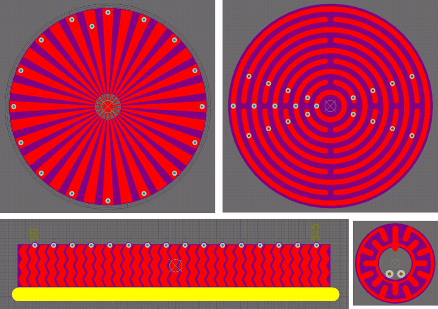
For complex shapes the Solid Region object is ideal, as a polygonal object it can be used to create virtually any shape. The following footprint was created by first setting the grid to suit the zig-zag requirements of the copper, and then placing one region object to give a single zig-zag shape. This was then copied the required number of times to define the copper area of the capacitive slider footprint. Alternating surface mount and through-hole pads were added on alternating ends of each zig-zag to define the connection points.
Use the Solid Region object to create unusual shapes needed in a pad.
Using Guides to Place a Region
If the pad shape requires a shape defined at specific locations that do not fall onto a grid, it can be more efficient to define linear or point guides, and then place on these guides. The animation below shows an wedge-shaped pad being created by:
- Defining 4 Point Guides at the required locations in the Guide Manager dialog,
- Disabling the Snap to Grid option and enabling the Snap to Guides options,
- Placing a Solid Region with corners on these Point Guides,
- Copying and pasting the Solid Region the required number of times, at the required angular intervals. The animation does not show placement of the pads, or the Solder Mask definition, which was done by placing a circle on the Solder Mask layer.
Brief animation showing the creation of a radial style set of custom pads, using Point Guides.
Converting an Outline to a Region
Another approach to defining an unusual pad shape is to first define a closed outline of the shape using lines and arcs, and then convert this outline to a Solid Region. The pads in the surface mount inductor footprint shown below were created using this approach.
The following steps were taken:
- Set the grid to suit the outer dimensions of the pad.
- Added 2 vertical and 2 horizontal guides to simplify the line/arc placement process,
- Defined a polar grid with the radial step set to suit the radius of the inner curve on the pad,
- Placed Line/Arc objects, as shown in the animation below,
- Placed an Arc, using the Heads-up display to set the radius and the horizontal Lines to snap the start and end points,
- Resized the horizontal Lines down to meet the ends of the Arc,
- Selected the Lines and Arcs, then ran the Tools » Convert » Create Region from Selected Primitives command,
- Edited the Region to set it to the Top Layer, and enable the Mask Expansion option,
- To finish the component, you would then copy and paste the Region to define the second pad shape, place a small pad in each Region to define a connection point in each pad, then add the Component Overlay.
Brief animation showning a custom pad being created by defining an outline, then converting that to a Solid Region.
Defining the Solder and Paste Mask
There are essentially 2 approaches for defining the solder and paste mask requirements for a custom pad.
- Use Altium Designer's calculated mask capability.
- Define the mask requirements manually by placing objects on the mask layer(s).
Calculated Masks
Any Altium Designer primitive object can have a calculated Solder and/or Paste Mask, which can either be a user-specified amount, or controlled by Altium Designer's rule system. This is achieved enabling the appropriate Mask Expansion setting in the object's dialog, as shown in the image below.
Enable the required Mask Expansion, selecting between from Rule or user-specified value.
Manually Defined Masks
When the mask opening requirements are not simply an expansion or contraction of the copper shape, it will not be possible to use a calculated mask. In this case you place suitable design objects on the required Mask layer. Keep in mind that the Solder Mask is defined in the negative, that is, the placed objects define openings in the Solder Mask layer. The following image shows a printed button that has the solder mask opening defined by a manually placed full circle arc, placed on the Top Solder Mask layer.
If the mask shape is more than an expansion/contraction of the pad shape, define the mask by placing objects to create the required shape.
Routing Connections for Custom Pads
Since Altium Designer is able to detect and resolve routing connections to any copper object, there are no specific limitations on how you route to a custom pad.
Thermal Connections for Custom Pads
Custom pads are often created for components that have larger, unusually shaped pads. If these pads need to connect to a surrounding polygon, you should consider the polygon thermal connection spokes during the design of the custom pad. Altium Designer uses the small pads included in the custom pad shape as the polygon connection points. To ensure the small pads are connected by spokes, position them close to the edge of the custom shape, such that the distance from the small pad edge to the edge of the custom shape, is less than half the polygon connection spoke width. Place a small pad for each polygon connection point required.
Include a small pad for each polygon connection point.
Acknowledgments
* Footprints courtesy of Dennis Saputelli, Integrated Controls, Inc.