Contents
- Defining Sheet Structure
- Building a Hierarchical Structure
- Top-Down Design
- Bottom-Up Design
- Mixed Schematic/HDL Document Hierarchy
- Maintaining Hierarchy
- Synchronizing Ports and Sheet Entries
- Renaming a Sheet Symbol's Child Sheet
- Supporting Multi-Channel Design
- Defining Net Connectivity
- Net Identifiers
- Negating Net Identifiers
- Setting the Scope for Net Identifiers
- Flat vs Hierarchical Connectivity
- Flat Designs Without a Top Sheet
- Connectivity Examples
- Example 1 - Hierarchical
- Example 2 - Ports Global
- Example 3 - Net Labels Global
- Example 4 - Net Labels and Ports Global
- Example 5 - Off-sheet Connectors
- Using Buses
- Navigating a Multi-Sheet Design
- Cross-Probing between Schematic and PCB
- Connectivity Insight
The structural and connective considerations involved in multi-sheet design are discussed, then the different browsing tools that let you verify net connectivity across source documents are described.
Engineers turn to multi-sheet design for various reasons, the primary one being project size; some projects are too large or complex to fit on a single sheet. Even when the design is not particularly complicated, there can be advantages in organizing the project across multiple sheets. For example, the design may include various modular elements. Maintaining these modules as individual documents would allow several engineers to work on a project at the same time. Another reason is that this method allows you to use small format printing, such as laser printers.
There are two decisions to make for each multi-sheet project - the structural relationship of the sheets and the method employed for electrical connectivity between circuitry on those sheets. Your choices will vary according to the size and type of each project and your personal preferences.
Defining Sheet Structure
While the project file links the various source documents into a single project, the document-to-document and net connective relationships are defined by information in the documents themselves. A multi-sheet design project is arranged as a hierarchical structure of logical blocks, where each block can be either a schematic sheet or a HDL file (VHDL or Verilog). At the head of this structure is a single master schematic sheet, more commonly referred to as the project's top sheet.
The sheet structure itself is formed through the use of a special symbol called a sheet symbol. Each of the source documents that constitute the design are represented on the top sheet by a sheet symbol. The Filename property of each sheet symbol references the schematic sub-sheet (or HDL file) that it graphically represents. In turn, a schematic sub-sheet can also contain further sheet symbols referencing lower schematic sheets or HDL files. In this way you can define a structural hierarchy of source documents that can be as simple or complex as your needs require.
When your multi-sheet project is compiled, the logical relationship of the design is realized and a structural framework is created. This is a tree structure, beginning with the schematic top sheet and branching down to include all other schematic sub-sheets and HDL files at one level or another.
Figure 1 shows two examples of compiled design hierarchy. On the left, the structural hierarchy for a compiled PCB design project (*.PrjPcb). On the right, the structural hierarchy for a compiled FPGA design project (*.PrjFpg).

Building a Hierarchical Structure
The design capture environment provides a range of features that allow you to build your multi-document, hierarchical structure quickly and efficiently. The exact features you choose to use depend on your personal design methodology - top-down or bottom-up.
It is important to remember that for hierarchical designs a project can contain only one top sheet; all other source documents must be referenced by sheet symbols. No sheet symbol may reference the sheet it's on, or any sheet higher up the ladder, as this will create an irresolvable loop in the structure.
Top-Down Design
The following commands are available that allow you to build the hierarchy of your design in a top-down fashion:
- Create sheet from symbol - use this schematic editor command to create a sheet below the nominated sheet symbol. Matching Ports will be added to the sub-sheet, ready to wire.
- Create VHDL file from symbol - use this schematic editor command to create a shell VHDL file, with an entity declared that includes port definitions to match the sheet entries in the nominated symbol.
- Create Verilog file from symbol - use this schematic editor command to create a Verilog file, with a module declared that includes port definitions to match the sheet entries in the nominated symbol.
- Push part to sheet - use this schematic editor command to "push" a placed part onto a new schematic sub-sheet, replacing the original part on the parent sheet with a sheet symbol pointing to the new sub-sheet. Matching ports will be added and wired to the part on the sub-sheet. Right-click on a component to access this command.
Bottom-Up Design
The following commands are available that allow you to build the hierarchy of your design in a bottom-up fashion:
- Design » Create symbol from sheet or HDL - use this schematic editor command to create a symbol from the nominated schematic sheet, VHDL file or Verilog file. Make the sheet that is to include the sheet symbol the active document before launching this command.
- Convert part to sheet symbol - use this schematic editor command to convert a chosen part into a sheet symbol. The symbol's Designator field will initially be set to the part's designator, with the Filename field set to the part's comment text. Change the filename to point to the required sub-sheet; change the sheet entries in accordance with the ports defined on that sub-sheet. Right-click on a component to access this command.
Mixed Schematic/HDL Document Hierarchy
When creating the design hierarchy, you can quite easily use a sheet symbol on a parent schematic sheet to reference a schematic sub-sheet below. This can be extended when capturing the design using a mixture of schematic sheets and HDL code. The VHDL or Verilog sub-documents are referenced in the same way as schematic sub-sheets, by specifying the sub-document filename in the sheet symbol that represents it.
When referencing a VHDL sub-document, the connectivity is from the sheet symbol to an entity declaration in the VHDL file. To reference an entity with a name that is different from the VHDL filename, include the VHDLEntity parameter in the sheet symbol, whose value is the name of the Entity declared in the VHDL file.
The process is similar when referencing a Verilog sub-document, where the connectivity is from the sheet symbol to a module declaration in the Verilog file. To reference a module with a name that is different from the Verilog filename, include the VerilogModule parameter in the sheet symbol, whose value is the name of the Module declared in the Verilog file.
Figure 2 illustrates an example of this mixed hierarchy, whereby the same sheet symbol has been used to reference a schematic sub-sheet in one instance of a design and an entity in a VHDL sub-document in another. In both cases, the sub-document implements the same circuitry (a BCD Counter).
Maintaining Hierarchy
Once you have defined the hierarchical structure of your multi-sheet design, you need to be able to maintain it. Altium Designer provides features that help you do just that.
Synchronizing Ports and Sheet Entries
A sheet symbol is 'synchronized' with its referenced child sheet below if all of its sheet entries match the corresponding ports on the sub-sheet - both by name and by IO Type. Use the Synchronize Ports to Sheet Entries dialog (Figure 3) to maintain the sheet symbol to matching sub-sheet links (select Synchronize Sheet Entries and Ports from the Design menu).
For detailed information on this synchronization process, refer to the Synchronizing Sheet Entries and Ports section of the Sheet Symbol topic. This topic can be quickly accessed by pressing F1 while the cursor is over a placed sheet symbol.
Renaming a Sheet Symbol's Child Sheet
During a design you may need to change the name of a schematic sub-sheet, for example you may have changed the circuitry on the sheet and require a different name to better reflect the sheet's functionality. Rather than rename the sheet and then manually change the reference for each sheet symbol that references the sheet, the Rename Child Sheet command is provided (accessible from the Design menu). With this command you can:
- Rename the child sheet and update all affected sheet symbols in the current design project
- Rename the child sheet and update all affected sheet symbols in the current design workspace (*.DsnWrk)
Create a renamed copy of the child sheet and update the current sheet symbol to point to it.
For detailed information on this renaming process, refer to the Renaming a Sheet Symbols' Child Sheet section of the Sheet Symbol topic. This topic can be accessed by pressing F1 while the cursor is over a placed sheet symbol.
Supporting Multi-Channel Design
The environment includes features specifically to support projects with repetitive circuitry - as well as the singular one sheet symbol = one sub-sheet representation, you can also create a structure where the same sub-sheet is referenced many times. This is known as multi-channel design.
There are 2 approaches to multi-channel design; by referencing the same sub-sheet from multiple sheet symbols, or using one sheet symbol with the Repeat keyword. When the design is compiled, any repeated sections (or channels) are automatically instantiated the required number of times. The advantage of multi-channel design is that it allows you to maintain a single copy of the source channel, even after the design has moved to implementation in the FPGA or on the PCB.
The syntax used involves the use of the Repeat keyword in the sheet symbol's Designator field and takes the form:
Repeat(SheetSymbolDesignator, FirstInstance, LastInstance), where SheetSymbolDesignator is the base name for the sheet symbol and FirstInstance and LastInstance together define the number of channels to be instantiated. It is important to remember that the FirstInstance parameter needs to start at a value equal to or greater than 1. Figure 4 illustrates the use of the Repeat keyword to instantiate 8 input channels for an audio mixer.
When the project is built, the Compiler instantiates the channel the required number of times as it builds the internal compiled model, using a chosen annotation scheme to uniquely identify each component in each channel. The channel sub-sheet is not duplicated. Instead, once compiled, a separate tab appears at the bottom of the sub-sheet document in the main design window, for each channel on that sheet, an example of which is shown in Figure 5.
The article Multi-Channel Design Concepts gives more information on how to capture a design with repeated sections.
Refer to the tutorial, Creating a Multi-channel Design for step-by-step instructions on building a multi-channel design.
Defining Net Connectivity
The only way to pass signals between sheets in a project is with net identifiers. These are objects that will make logical connections with one another, rather than physical connections (wires). Of course, net identifiers can also be used locally within a single sheet, as shown below.

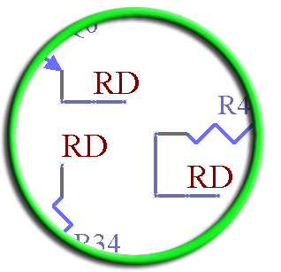

These pictures show how wires can be replaced by net labels, ports and power ports, respectively. These are known as net identifiers, and will be discussed in detail in the next section.
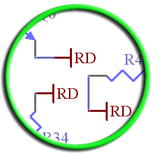
The pictures below illustrate a common misconception: that net identifiers of different types (such as net labels and ports) will connect logically if their names match. In fact, the opposite is true: different kinds of net identifiers may have distinct names, but still be wired together to form a single net.
These diagrams are all concerned with net identifiers replacing physical connections within a single sheet. What they do not show is that net identifiers give you the freedom to transfer nets between sheets in a multi-sheet project. How this happens depends upon the net identifiers used in your design, and the setting of the Net Identifier Scope.
Net Identifiers
The most basic net identifiers are net labels. Their primary function is to name a net, and to also alleviate the traffic of wire connections within a sheet. While there are ways and circumstances in which net labels can be made to correspond between sheets, you should generally consider them for local (within-sheet) connections.
Ports, like net labels, will always connect locally to matching ports on the same document. Unlike net labels, ports are specifically designed for inter-sheet connections. This can happen horizontally or vertically. Horizontally is the broadest option, as it disregards your multi-sheet structure and connects all ports with the same name across all sheets in your project. Hierarchical connections are more controlled, as they connect signals vertically between the sub-sheet and the parent sheet only. Instead of matching ports with ports, vertical connections are made between a port on the sub-sheet and a sheet entry on the parent sheet. This sheet entry must be placed within the sheet symbol referencing that specific sub-sheet.
Off-sheet connectors allow you to create horizontal connectivity for a select group of sheets within your project. The way to group these sheets is by placing multiple sheet names in the Filename field of a single sheet symbol, separating each with a semi-colon. Now place off-sheet connectors for those signals that must be carried between these grouped sheets. Off-sheet connectors will connect with matching off-sheet connectors, but only within those sheets grouped together on the parent sheet symbol. If only one sub-sheet is designated by a sheet symbol, then its off-sheet connectors will not connect to matching ones that may exist elsewhere in your project.
Power ports (also called power objects) completely disregard the structure of the project, and connect to matching power ports through all linked sheets. Hidden pins can be made to do this same thing by entering a value in the Connect To field (in the Pin Properties dialog). If you are importing a design from Protel 99 SE or earlier, any hidden pins will have a net name placed in this field automatically.
Table 1. Summary of the different Net Identifiers
| Net label | always connects to net labels of the same name within a sheet. Can also be used to connect horizontally between sheets if the Net Identifier Scope is set to Global. |
| Port | connects vertically if it is matched to a sheet entry on the parent sheet symbol and either the Hierarchical or Automatic Net Identifier Scope is used. It connects horizontally to all matching ports when either the Flat or Global scope is used. |
| Sheet Entry | always connects vertically down to a port on the sheet referenced by the symbol. |
| Off-sheet Connector | connects horizontally to matching off-sheet connectors in flat designs, otherwise they are limited to sheets referenced within a single, "sub-divided" sheet symbol. Note: Port Cross-References cannot be applied to off-sheet connectors, therefore Ports should be used where possible. |
| Power Port | connects globally to all matching power ports across your entire project. |
| Hidden Pin | connects globally to all hidden pins in your project that have a matching Connect To value. |
For detailed information on Net Labels, Ports, Sheet Entries, Off-Sheet Connectors and Power Ports, press F1 while the cursor is over one of these placed objects.
Negating Net Identifiers
Should you need to negate (include a bar over the top of) a net label, sheet entry or port, this can be done in one of two ways:
- Include a backslash character after each character in the net name (e.g. E\N\A\B\L\E)
- Enable the Single '\' Negation option on the Schematic - Graphical Editing page of the Preferences dialog, then include one backslash character at the start of the net name (e.g. \ENABLE).
Setting the Scope for Net Identifiers
The connectivity that is created when you compile a multi-sheet project depends on the scope of the net identifiers. The scope specifies how you want the net identifiers to connect: Flat – ports connect globally between all sheets; Global – ports AND net labels connect globally between all sheets; Hierarchical – connections are only created vertically (sheet symbol to sub-sheet) between a port and the matching sheet entry.
You define the connectivity by setting the Net Identifier Scope in the Options tab of the Options for Project dialog (Project»Project Options). As well as the 3 options mentioned above (Flat, Global, Hierarchical), there is also an Automatic option. Generally it is better to leave the Scope set to Automatic, Altium Designer will select the most appropriate of the 3 options based on the structure of the sheets and the presence/lack of Ports and Sheet Entries.
There are two special net identifier objects that are always deemed to be global: power ports and hidden pins. The connective behavior of Off-sheet connectors always operate in the same way, regardless of the Net Identification Scope.
Flat vs Hierarchical Connectivity
In terms of document structure, all multi-sheet design projects are organized hierarchically, even if the hierarchy is limited to only two levels (i.e. a top sheet containing all sheet symbols that reference the sub-sheets on the level below). In terms of connectivity, a design can follow either a 'flat' or hierarchical' structure. The base difference between the two is that hierarchical designs relay signals between sheets according to the sheet structure you have created, while flat designs take no consideration of the structural arrangement of sheets.
It is important to note that when designing an FPGA project, the connective model employed must be hierarchical.
Flat Designs Without a Top Sheet
If your design is not hierarchical - i.e. the sub schematic sheets are all on the same level, with no sheet symbols referencing further sheets below - the design is a flat one. In this case, you are not required to have a top sheet, containing only sheet symbols to reference those sheets below. The requirement for a top sheet dates back to when there was no project file, without a project file the software had to rely on the sheet symbols on the top sheet to determine which sheets were in the project. To test such a project without a top sheet, right-click on its filename in the Projects panel and choose Remove from Project from the context menu.
Flat design projects that already include the top sheet will compile correctly, but Altium Designer gives you the choice to build your project without a top sheet, should you wish.
Connectivity Examples
The following four illustrations will show how the detected or selected scope will affect the connectivity of net labels and ports in the same inter-sheet structure. The fifth shows how off-sheet connectors work.
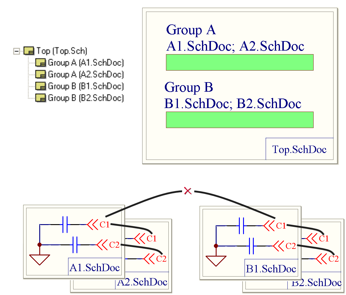
Example 1 - Hierarchical
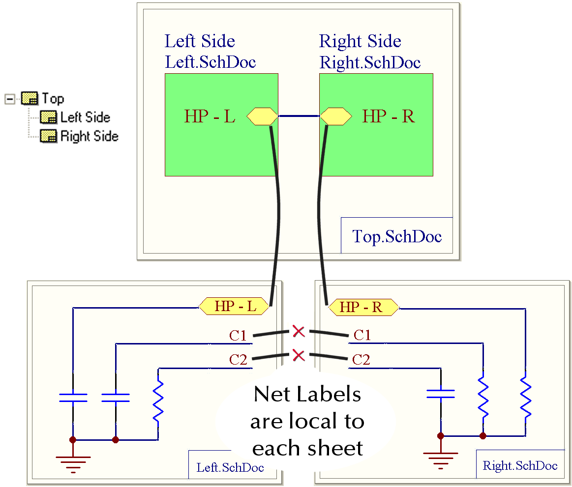
This schematic project will automatically be detected for hierarchical scope, due to the presence of sheet entries within the sheet symbols on the parent sheet. The net labels C1 and C2 on each sub-sheet will not connect to matching net labels on the other sub-sheet, but remain within the confines of their local sheets. The ports in this example have different names, but even if they had matching names, they would not make horizontal connections with one another between sub-sheets when the hierarchical scope was in effect. Instead, ports will only make trans-sheet connections vertically, up to the parent sheet. For this to work, the port on the sub-sheet must find a matching sheet entry inside the corresponding sheet symbol. That connection may then be wired to pins or other net identifiers from the sheet entry on the parent sheet.
In this example, the sheet entries on the parent sheet are connected to one another (notice that their names do not match; this is a physical connection, not a logical one). In a more highly-developed structural design, these signals could have been wired to ports and matched to entries within another sheet symbol on a grand-parent sheet.
Example 2 - Ports Global
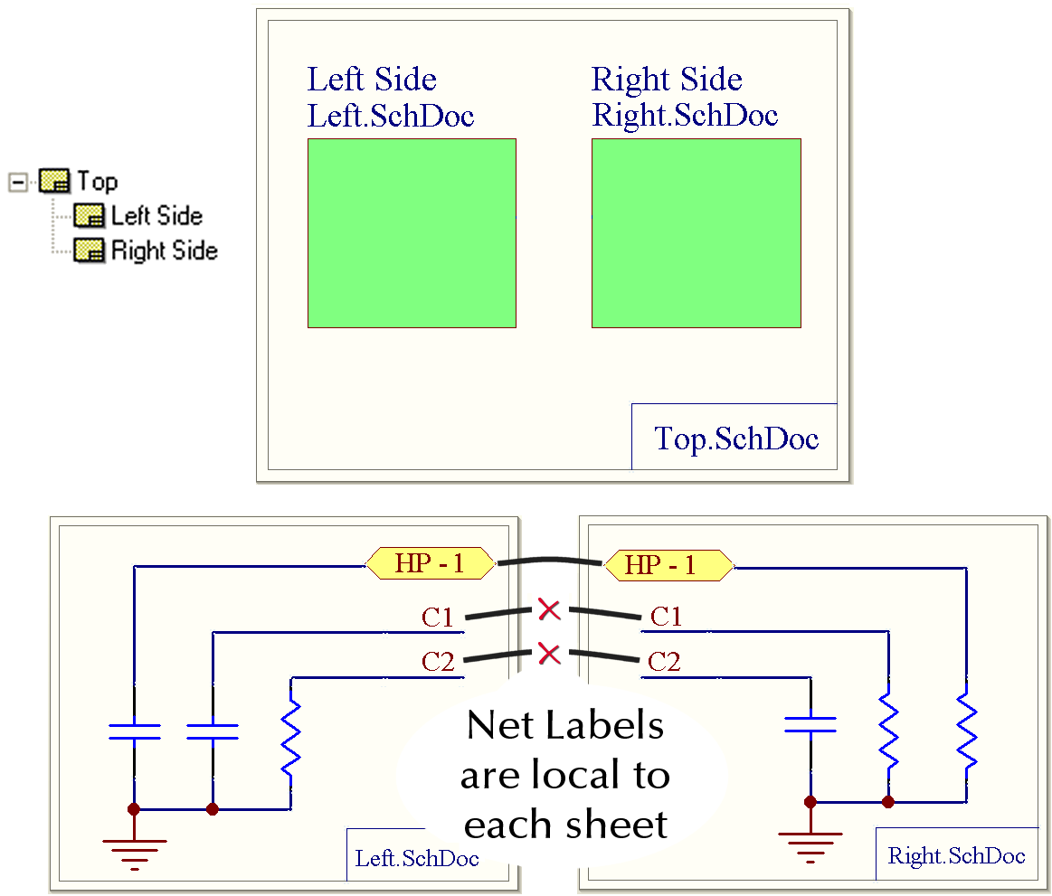
The presence of ports in this design, along with the absence of any sheet entries, causes the scope to automatically change to ports global. This essentially flattens the project as far as ports are concerned; they will make logical connections to all ports with matching names anywhere in the project. Net labels do not share this same ability; they will remain local to individual sheets.
As this design project is flat, the top-sheet could be removed from the project and the design would still compile correctly. Remember, Altium Designer uses the project file to determine which sheets are in the design project.
Example 3 - Net Labels Global
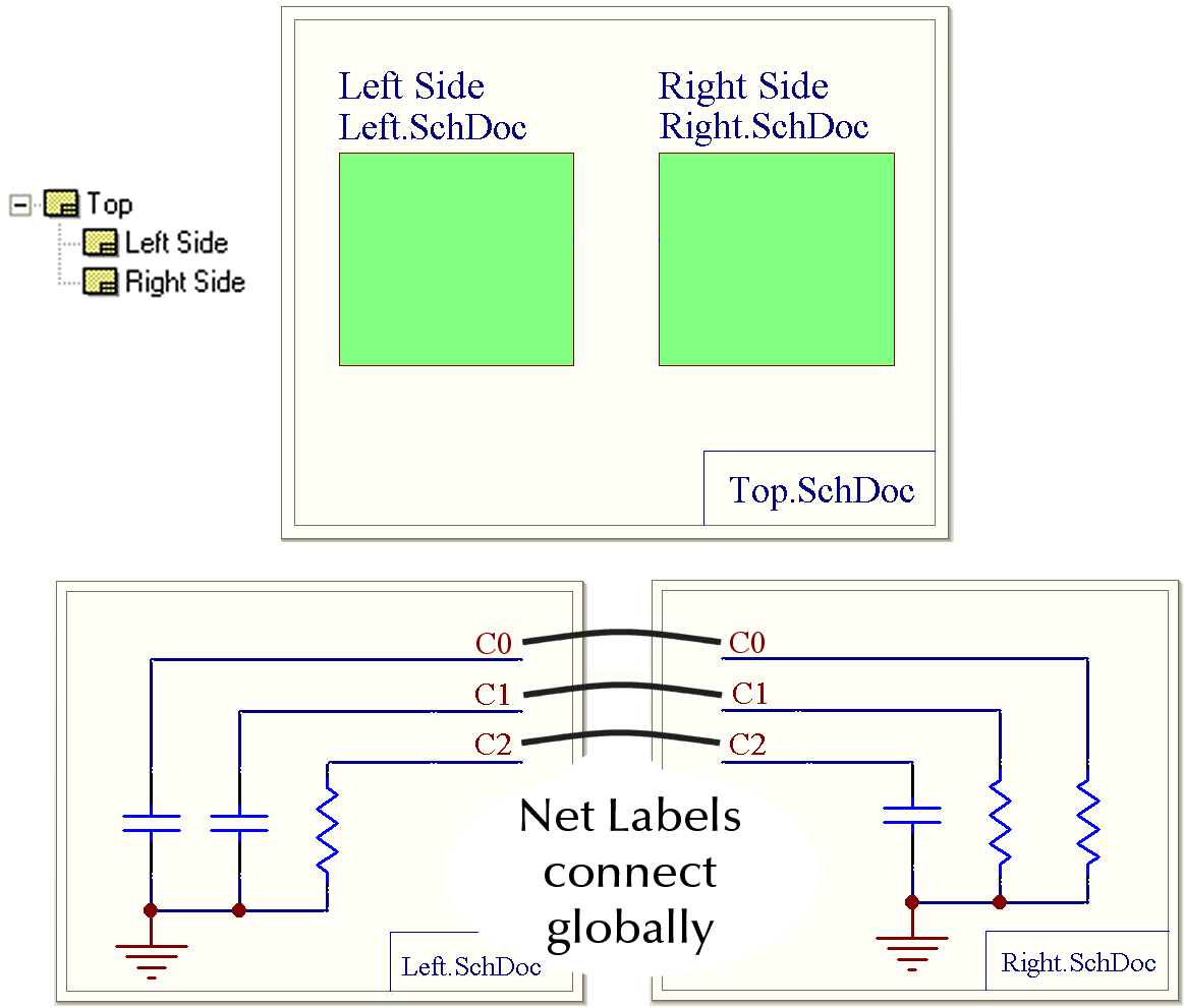
This project is entirely devoid of both sheet entries and ports. This is the only case in which net labels will automatically make global connections in a multi-sheet design. These net labels will connect with all matching net labels in the project, regardless of the structure.
Again, as this design project is flat, the top-sheet could be removed from the project and the design would still compile correctly.
Example 4 - Net Labels and Ports Global
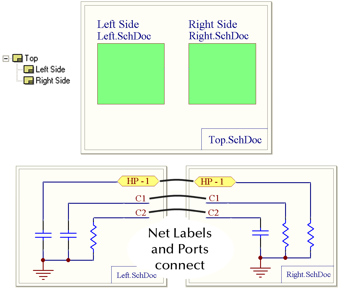
This scope is not available through automatic detection, but has been continued in Altium Designer to provide support for legacy designs. In it, both net labels and ports make global connections with matching net identifiers in a horizontal fashion. The only way to achieve this kind of connectivity is to browse to the Options tab of the Options for Project dialog, and change the Net Identifier Scope to Global (Netlabels and ports global).
As this design project is flat, the top-sheet could again be removed from the project and the design would still compile correctly (the project file itself holding the information about which source documents form the design).
Example 5 - Off-sheet Connectors
It is important to remember that although there are times when an Offsheet connector and a Sub-divided Sheet Symbol can be useful, they do have limitations. They will not properly form automatic room definitions and component classes and these need to be recreated manually in the PCB if you choose to use them.
In this example, the top sheet references four sub-sheets with only two sheet symbols. This is done by referencing multiple schematic files in the sheet symbol's Filename field, separated by a semicolon. Off sheet connectors will then create flat connections between all sheets grouped within a single sheet symbol - even if other sheets in the project are using vertical connectivity.
The grouping of sheets has no effect on any net identifiers except for off-sheet connectors. It creates a haven within your design that can accommodate flat connections - but this will only occur between matching off-sheet connectors. Notice how these connections are maintained within groups only. They do not cross into other groups, even if they contain off-sheet connectors with matching names.
Many designers may never use off-sheet connectors. They were introduced primarily as a means of importing designs seamlessly from other design packages.
Using Buses
Many schematics contain buses, which symbolize grouped signals. They are conventionally drawn with a greater thickness than wires, making them easy to identify. This graphical aspect of buses can be a useful tool in itself, but bused signals can also be transferred between sheets, according to the general rules of connectivity described previously.
The example circuitry in Figure 6 above contains four buses: two graphical and two logical. Logical buses are attached to net identifiers (net labels and/or ports) which use bus syntax. To understand bus syntax, consider one of the logical buses in this example more closely:
These eight nodes are eligible for inclusion in a bus because they have net labels that share the same prefix, followed by a numeric suffix. The logical bus is created by a net label with the syntax D[0..7], where D is the shared prefix, and the numbers 0 and 7 mark the smallest and largest numbers in the suffix. Any non-negative numbers can be used in this suffix, and the order is only important so long as it agrees with any other net identifiers on the same bus. For example, we could change the net label D[0..7] to D[7..0], so long as we also changed the order both in the attached port and in the sheet entry it matches on the top sheet of this design.
It is recommended that the net label's prefix does not end with a number, for example, Headphone[1..8] netlabel where the Headphone prefix only has alpha characters. The Headphone1[1..8] netlabel has a number 1 at the end of the prefiix which expands to Headphone11..Headphone 18, which can cause net naming conflicts in your design.
Notice that the logical bus is created by the net label, not the bus primitive. The electrical function of the bus is to connect these net identifiers. Remember that net identifiers of different types do not automatically connect to one another, even if they share the same name. This holds true for net identifiers with bus syntax; a net label D[0..7] will not automatically connect to a port with the same name. The bus is required to connect them together.
The rest of the bus - that portion which extends towards the individual nets, is important for graphical reasons only. Bus entries have no connective properties, but provide a clearance around buses which might be fed by wires on either side (two wires touching a bus at the same point would short together).
The two buses in the example schematic which are entirely graphical do not touch any net identifiers. In this case, the actual connections will be made between matching net labels. Deleting such buses would have absolutely no effect upon the connectivity of your sheet (although it would make the schematic harder for humans to read).
The nets in this example are, in fact, ineligible for logical bus connectivity, because their names do not conform to the requirements of the bus syntax. Remember that all nets in a single bus must be individually labeled with the same prefix, and be distinguished from one another by their numeric suffix alone.
Navigating a Multi-Sheet Design
See Navigator to learn about the center-piece for net connectivity in your design
Use the Up/Down Hierarchy feature, accessed by clicking on the ![]() button, to navigate up or down through the design hierarchy. If you click on a sheet entry you will be presented with the matching port on the sub-sheet, if you click on a sheet symbol you will be presented with the entire sub-sheet. To navigate up through the hierarchy, click a port to be presented with the matching sheet entry on the parent sheet.
button, to navigate up or down through the design hierarchy. If you click on a sheet entry you will be presented with the matching port on the sub-sheet, if you click on a sheet symbol you will be presented with the entire sub-sheet. To navigate up through the hierarchy, click a port to be presented with the matching sheet entry on the parent sheet.
Hierarchy can also be navigated directly by pressing Ctrl and double-clicking over a port, sheet entry or sheet symbol.
Cross-Probing between Schematic and PCB
Since designing a PCB from a schematic project is a highly iterative process, the Navigator panel also allows cross-probing between schematic and PCB documents. Open the PCB document, and hold down the Alt key while navigating objects on the schematic source - the same highlighting options will apply to both the navigated schematic objects and the corresponding PCB objects.
You will find that cross-probing through the Navigator panel is a little bit different than using the cross-probe command in the Tools menu. The latter command is available in both schematic and PCB environments, while the Navigator panel's tools are designed to start in the schematic portion of the project. The cross-probe tool does not apply the current highlighting settings to the document you're probing---only the destination document that responds. Finally, the cross-probe tool offers jump-probing, done by holding the Ctrl key when probing an object. This is different from the Navigator panel's tools, which will apply highlights to the PCB, but will not make it the active document.
Connectivity Insight
For more information about Connectivity Insight see Design Insight